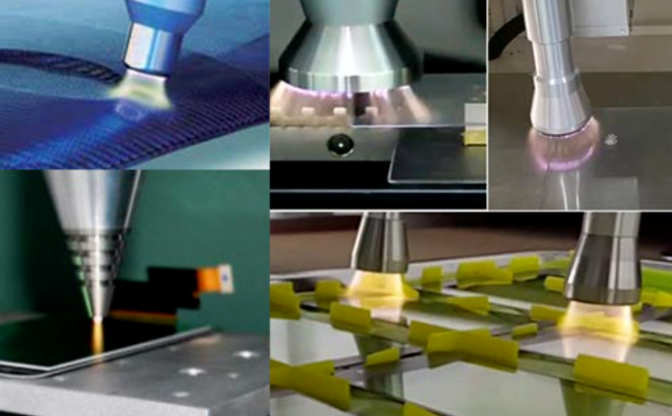
Plasma cleaning is driving a new development and transformation in the semiconductor industry. It provides enhanced cleaning, surface modification, and advanced etching processes. By utilizing ionized gas, this method not only removes pollution with incredible efficiency, but also controls surface conditions to improve adhesion.
From manufacturing to semiconductor development, various industries are realizing the benefits of highly active ions and molecules in plasma. These ensure that the surface is not only perfectly clean, but also optimized for specific applications. In this article, we will explore plasma treatment and its indispensable role in the semiconductor industry.

What is plasma cleaning
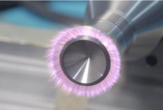
Plasma cleaning is defined as the process of using ionized gas to interact with a substrate to remove contamination and modify its surface
Plasma cleaning is not only a cleaning process, but also a surface modification and etching process. More broadly, we can say that most plasma cleaning applications promote adhesion between two objects by:
Purification of their contact surfaces
Generate improved surface conditions, such as increasing surface roughness
Increase surface energy
Make the surface hydrophilic
Make the surface hydrophobic (non hydrophilic)
Removing metal oxides through physical and/or chemical interactions
The main applications of plasma cleaning
One of the main applications of plasma treatment is surface cleaning. During this process, plasma is used to effectively remove pollutants from the surface of materials. Due to its effectiveness and efficiency, it is a popular cleaning method in many industries. Highly active ions and molecules in plasma can decompose organic pollutants and residues, resulting in clean and pure surfaces.
Surface activation is another common application. In this process, plasma treatment is used to increase the surface energy of the material to improve adhesion. This is particularly useful in the bonding, painting, and coating of materials, as enhancing adhesion can improve the quality and durability of the final product.

Plasma treatment can also be used for surface coating. In this method, plasma is used to coat coatings that can protect, enhance, or modify the surface properties of materials. It ensures a uniform coating and can be used for various purposes, including improving wear resistance, corrosion resistance, and environmental impact.
Plasma cleaning in the semiconductor industry
Plasma treatment is widely used in a range of applications, including cleaning, etching, and deposition processes. These processes are crucial for the manufacturing and development of semiconductor devices such as integrated circuits (ICs), microelectromechanical systems (MEMS), and other nanoscale devices.

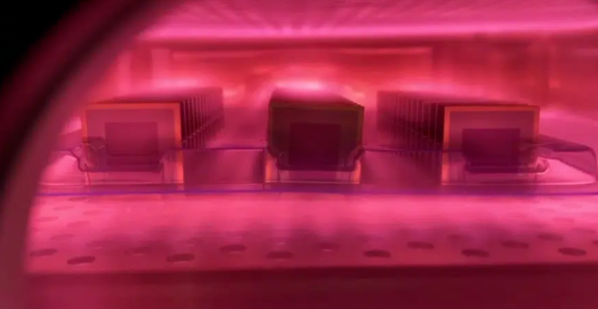
Plasma cleaning is used to remove organic and inorganic pollutants from the surface of semiconductor wafers. By combining active ions and ultraviolet radiation, plasma cleaning effectively eliminates residues, ensuring a clean and defect free surface. This is very useful when analyzing the semiconductor industry.
Plasma etching is one of the most critical applications in semiconductor manufacturing. This is a process of removing selective materials from the surface of a wafer, leaving clearly defined patterns that are an essential part of the functionality of semiconductor devices.
Plasma treatment can achieve high control and create complex patterns and structures with extremely high precision. This is an efficient process that is crucial for achieving the cleanliness and mode resolution required for semiconductor manufacturing. By using different gases and precise control of process parameters, the surface properties of materials can be extensively modified.
Case 1: Plasma cleaning and wire bonding yield rate
In the semiconductor industry, a typical application is to clean the surface of lead frames and the molds mounted on them with plasma. This is usually done before the wire bonding process to improve bonding efficiency. It is also carried out before the molding process to ensure the elimination of voids and delamination, thereby improving the yield rate.
The semiconductor manufacturing process aims to manufacture each individual chip to perform according to specifications. However, manufacturing issues during the processing, changes in process variables, and cross contamination from other processes may cause some molds to fail due to NSOP (non stick to solder pads) phenomenon.
The event of unsuccessful NSOP bonding (no adhesion between the welding wire and the mold pad surface) was effectively controlled through plasma cleaning.

Case 2: Surface pretreatment
In the electronics and semiconductor industries, surface treatment is a key step in wire bonding and packaging yield, and plasma treatment plays a crucial role in ensuring the effective implementation of these processes.
Wire bonding is a method of connecting semiconductor devices to their packaging, which involves using thin wires to establish electrical connections. During this process, surface preparation is essential to ensure surface cleanliness, absence of contaminants, and sufficient activation to promote strong adhesion between wires and semiconductor devices.
This surface pre-treatment is very important because any contamination on the surface can seriously hinder the wire bonding process. Pollutants can cause poor adhesion. The uniform surface ensures consistent wire bonding effect, reduces variability, and improves the overall reliability of semiconductor devices.
Case 3: Bond yield issue
An example of how plasma cleaning can help solve problems comes from an experiment in which a gold coated palladium bonding pad was developed to reduce surface pits on silicon. This component exhibits a high bonding failure rate due to the presence of surface oxides while increasing its hardness. To reduce or eliminate these oxides, Ar/H2 plasma is used to form hydrogen radicals and undergo chemical reactions with metal oxides. Compared with pure argon ion bombardment, Ar/H2 is more effective and faster in removing metal oxides.
In short, this bonding pad made of gold-plated palladium should be very strong, but due to the presence of surface oxides (compounds similar to rust), it has a high rate of bonding defects. In the experiment, a mixture of argon and hydrogen is converted into plasma, which is a pressurized gas that can clean and modify surfaces. This plasma mixture helps to effectively remove surface oxides. When using this plasma mixture to clean solder pads, the problem of poor wire bonding is significantly reduced.

Case 4: Improving Bonding Quality
As mentioned earlier, plasma cleaning can greatly alter the surface of metal substrates or chip PADs. By effectively eliminating the problem of poor wire bonding, plasma cleaning can effectively improve the yield of wire bonding products.
Using plasma cleaning to prepare the surface of chips and lead frames will increase the adhesion of this specific component, while easily removing organic pollutants or oxides left by previous process steps, which is a win-win situation.
After using ion cleaning technology, both bonding force and shear force will increase, resulting in more reliable bonding and improving the overall performance of the product.
Plasma cleaning, with its various functional advantages, is reshaping the semiconductor industry. It improves the reliability of semiconductor devices and makes certain processes simpler and more efficient. As more and more industries tap into its potential, the application of plasma cleaning is sure to play a greater role in the semiconductor industry.
Disclaimer: This article is reproduced or adapted online, and the copyright belongs to the original author. The content of the article is the author's personal opinion. Reproduction is only intended to convey a different viewpoint and does not represent the company's endorsement or support of that viewpoint. If you have any objections, please feel free to contact us.