Source: official account: comprehensive research on optics and semiconductors

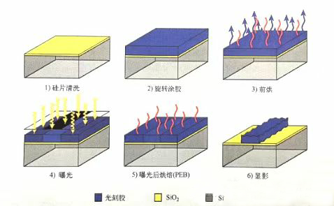
Let's first take a look at a typical photolithography process flowchart. On top of the silicon wafer is a SiO2 layer. Firstly, chemical or mechanical methods are used to remove pollutants from the surface of the silicon wafer. After cleaning and surface pretreatment steps, a bottom film treatment is carried out using a thickening agent to enhance the adhesion of the photoresist. Afterwards, the liquid-phase photoresist is spin coated onto the surface of the silicon wafer using a spin coating method, with a photoresist thickness generally ranging from 50nm to 1um. The thickness of photoresist can be adjusted by adjusting the rotational speed and photoresist viscosity. Pre baking is the first baking step, which mainly removes solvents from the photoresist and improves the adhesion between the silicon wafer and the photoresist. Exposure is the process of transferring the image generated by a projection lithography machine into a photoresist. Based on the distribution of the transparent area of the mask, certain regions of the photoresist are exposed, and the properties of the photoresist in the exposed area change. In general, the exposed photoresist needs to undergo another baking process, namely post exposure baking (PEB). The implementation of PEB mainly depends on the type of photoresist and other process requirements. Some photoresists require PEB to trigger certain important chemical reactions. In addition, PEB can completely remove solvents and accelerate the diffusion of substances inside the photoresist, smoothing the outline of the photoresist. Finally, immerse the exposed and locally chemically modified photoresist in a developing solution for development. The development result depends on the polarity of the photoresist. The exposed and chemically modified parts of the positive gel are removed during the development process, while the negative gel is the opposite, and the unexposed areas are removed by the developer. When performing subsequent etching and doping treatments on the material layer under the photoresist, the developed photoresist pattern serves as a mask.
photoresist
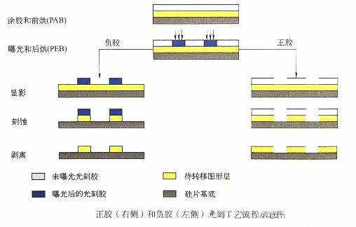
The polarity, thickness, optical properties, chemical composition, and reaction mechanism to incident light of different photoresists are all different. After exposure, the solubility of positive photoresist will increase, while the solubility of negative photoresist will decrease. During the chemical development process, the highly soluble parts of the photoresist are developed, and the remaining photoresist serves as a mask for etching or doping processes. The following diagram shows the process flow of positive and negative adhesive technology. The starting point for both processes is photoresist spin coating and first baking (PAB, also commonly known as pre baking). Exposure and post exposure baking (PEB) can alter the solubility of the photoresist exposed area. According to the polarity of the photoresist, chemical development washes away the exposed portion (positive photoresist) and unexposed portion (negative photoresist) of the photoresist. The remaining photoresist is used as a mask for selective etching, implantation, deposition, and other processes, and finally the photoresist is peeled off. The patterns formed by positive or negative glue processes complement each other.

The solubility of photoresist in the developing solution can be changed according to different mechanisms.
Change polarity: Most modern photoresist systems contain a functional group that can change polarity. The wavelength range suitable for DNQ photoresist is between 350nm and 450nm, and it converts alkali insoluble molecules into alkali soluble molecules through light induction. Advanced positive chemical amplification photoresists (CARs) use acid catalyzed deprotection reactions to convert lipophilic polymer groups into hydrophilic groups.
Aggregation and depolymerization: Light induced intermolecular reactions can generate long chains that can damage the polymer. Most photoresist systems utilize photoinitiators to activate the polymerization reaction of functional groups. Adding quencher molecules to photoresist materials can control the diffusion of polymerization reactions. The polymerization and depolymerization reactions of monomers can affect the average molecular weight and solubility of materials. Free radical polymerized photoresist is commonly used in laser direct writing lithography. SU-8 photoresist is a typical negative polymer material with high transmittance in the ultraviolet spectral range, making it suitable for thick photoresist processes, especially in applications such as microelectromechanical systems (MEMS), micro optics, and microfluidics.
Crosslinking: Activated substances generated by radiation trigger the formation of bonds between linear polymer chains, leading to cross-linking. Crosslinking changes the molecular size of different regions and affects the average molecular weight of polymer materials. The three-dimensional network structure of the generated polymer is called gel. A certain exposure dose is required to start the gel process, which is the gelation point. The light induced gel reaction will reduce the solubility of the materials. Hydrogen sesquioxane (HSQ) is this type of photoresist. Unlike many negative photoresist based on polymerization reactions, this type of photoresist does not expand.
Main chain breakage: In the wavelength range below 250nm, the energy of photons/particles exceeds the binding energy of C-C bonds in photoresist, so photo induced main chain breakage can be used to improve the solubility of photoresist in the exposed area. Taking PMMA (polymethyl methacrylate) as an example, although it has high resolution, its corrosion resistance and sensitivity are poor, which limits the application space of this material. There are many positive photoresists based on chain breakage, such as PBS (Polyvinylsulfone), SNS (Sulfone Phenolic Resin System), etc., which are commonly used in electron beam lithography.
Photoisomerization: The structural transformation between isomers can be triggered by photoexcitation. Isomers are molecules with the same number of atoms but different arrangements for each element. The latest research on azo polymers shows that there are several new entry points for the application of photoisomerization in nanographic technology, especially in photon applications. The structural changes of azo polymers are very sensitive to the polarization state of incident light, and may become a technical approach to achieve polarization sensitive photoresists.
Light doping: This technology uses a double-layer system composed of a sulfur-containing glass film (such as As2S3) and a metal containing film on top. Exposure of certain areas of the metal film results in photo induced metal migration, causing the metal to migrate into the sulfur based glass. The migration of metals increases the solubility of sulfur based glasses in alkaline solutions. This phenomenon can be utilized to achieve high-precision positive graphic transfer. The lateral diffusion of metal from the unexposed area to the exposed area and photobleaching can further sharpen the edges of the graphic and improve contrast. However, there is a high risk of metal ion and atomic contamination during light doping, and some sulfur based compound photoresists are highly toxic.
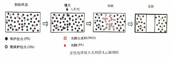
The photoresist can be chemically amplified (or not amplified). Chemical amplification of photoresist will generate catalysts after exposure, which act on surrounding molecules, triggering cascade reactions or chain reactions that alter the solubility of photoresist. Chemical amplification improves the sensitivity of photoresist to incident light, and all standard photoresists with exposure wavelengths of 248nm and 193nm are chemical amplification photoresists. Here we will focus on introducing the currently advanced positive chemical amplification photoresist. The photoresist used in DUV lithography with an exposure wavelength less than 300nm is chemically amplified photoresist (CAR). The chemical amplification photoresist with a typical exposure wavelength of 248nm is composed of sparsely distributed photoacid generators (PAGs) such as PHOST based polymers and onium salts. After exposure, the photoacid generator will generate photoacid. A photoacid molecule can catalyze multiple deprotection reactions, thereby altering the solubility of surrounding polymers. The transmittance of aromatic polymers such as PHOST at 193nm wavelength is insufficient. Therefore, ArF lithography uses chemical amplification photoresists such as acrylic esters and ester protected cyclic polymers. The evolution process of the chemical state of positive chemical amplification photoresist during the photolithography process is shown in the following figure. In the initial state before exposure, high concentration protective sites are uniformly distributed in the photoresist. Protecting the sites makes the photoresist material insoluble in the developer solution. At this point, the photoacid generator (PAG) is sparsely distributed within the photoresist. After the incident photons collide with PAG, photoacid is generated, which increases the concentration of photoacid in the transparent area. The incident light will not directly affect the concentration of protective sites. The photoacid triggers a catalytic reaction, causing the adjacent protective sites to lose their protective function. Most chemical amplification photoresists are high activation energy photoresists, and the catalytic deprotection reaction of these materials only occurs during the baking process after exposure. In addition to high activation energy photoresist materials, there are some low activation energy photoresist materials outside the sea. In low activation energy materials, the deprotection reaction does not require energy provided by post baking heating. After development, the areas with low concentration of protective sites in the photoresist are washed away.

Chemical amplification makes materials and processes highly sensitive to small changes in acid concentration. The acid molecules generated by a small exposure dose are sufficient to alter the solubility of photoresist. The high photosensitivity of chemically amplified photoresist improves the yield of lithography projection systems, which increases the number of silicon wafers exposed per hour.
Reference: "Lithography Theory and Technology"
*Disclaimer: The content of the article is the author's personal opinion. Reproduction on the website is only intended to convey a different viewpoint and does not represent the company's endorsement or support of that viewpoint. If you have any objections, please feel free to contact us.