Source: Content compiled by Semiconductor Industry Watch (ID: icbank) from tomshardware
ASML announced at IMEC's ITF World 2024 conference that its first high numerical aperture machine has now set a new chip manufacturing density record, surpassing the record set two months ago. Martin van den Brink, former president and chief technology officer of ASML, currently serves as a consultant at the company. He also proposed that the company could develop hyper NA chip manufacturing tools to further expand the scale of its high NA machines and shared a potential roadmap.
He outlined a plan to significantly increase the speed of future ASML tools to 400 to 500 wafers per hour (wph), which is more than twice the current peak of 200 wph, in order to reduce EUV chip manufacturing costs. He also proposed a modular unified design for ASML's future EUV tool series.
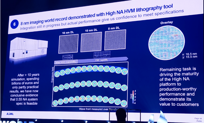
Van der Brink stated that after further adjustments, ASML has now used its groundbreaking high numerical aperture EUV machine to print 8nm dense lines, which is the density record of machines designed specifically for production environments. This broke the record set by the company in early April, when it announced that it had printed 10nm dense lines using a groundbreaking high NA machine located at ASML headquarters in Feldhoven, the Netherlands, in collaboration with imec laboratory.

In the long run, ASML's standard low NA EUV machine can print critical dimensions of 13.5nm (CD - the smallest feature that can be printed), while the new High NA EXE: 5200 EUV tool aims to manufacture smaller transistors by printing 8nm features. Therefore, ASML has now proven that its machines can meet its basic specifications.
Today, we have made progress in displaying record breaking 8nm imaging, corrected across the entire field of view, but with some degree of overlap, "Van der Brink said." By the way, this is not perfect data, but it's just to show you progress. Today, we are confident that with High NA technology, we will be able to cross the finish line in the future

This milestone represents the result of over 10 years of research and development and billions of euros in investment, but there is still more work to be done to optimize the system and prepare for large-scale production by major chip manufacturers. This work has already begun in the Netherlands, and Intel is the only known chip manufacturer that has fully assembled the High NA system. It is following in ASML's footsteps and operating its own machines at the D1X factory in Oregon. Intel will first use its EXE: 5200 High NA machine for research and development purposes, and then put it into production at the 14A node.

Van der Brink has once again proposed a new ultra numerical aperture EUV machine, but a final decision on the machine has not yet been made - ASML seems to be weighing industry interest, but only time will tell whether it will be realized.
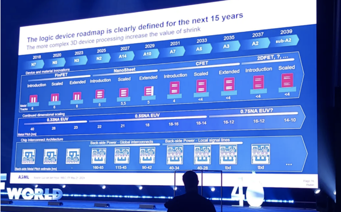
The current standard EUV machines use light with a wavelength of 13.5nm and a numerical aperture (NA - a measure of the ability to collect and focus light) of 0.33. In contrast, the new high numerical aperture machine uses the same wavelength of light but employs 0.55 NA to print smaller features. The hypernumerical aperture system proposed by Van der Brink will once again use light of the same wavelength, but expand the NA to 0.75 to enable printing of smaller features. We are not sure about the proposed critical size, but the timeline of the ASML transistor above shows that it is intercepting and extending to 10nm (nodes below A2) at the 16nm metal spacing (A3 node).

According to the above roadmap, Hyper NA may be suitable for single exposure 2DFET transistors, but it is currently unclear whether using High NA and multiple exposures can also produce such fine spacing.
As you can see in the first slide above, this machine will not be available until around 2033. Today's High NA machines have already cost approximately $400 million. Due to the need for larger and more advanced mirrors and improved lighting systems, Hyper NA will be a more expensive option.
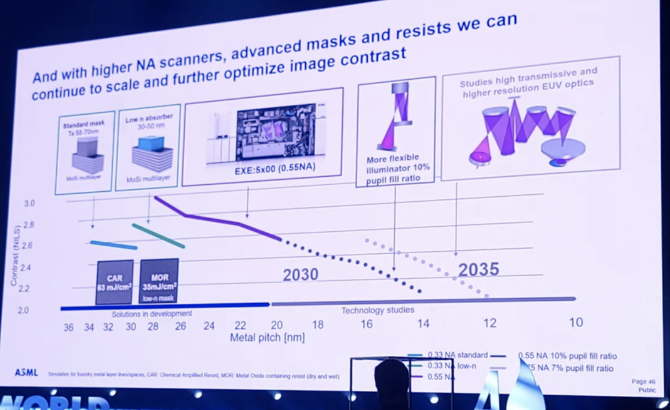
Like its predecessor, the goal of Hyper NA is to print smaller features with a single exposure, avoiding multiple exposure techniques (multiple exposures of the same area) that often increase the time and steps of the chip manufacturing process, as well as the possibility of defects, all of which increase costs. Van Der Brink stated that continued development of lithography machines and advanced masks will be key to improving the resolution of printed features. Hyper NA will also use an improved lighting system to achieve optimal results. ASML did not provide a detailed explanation, but it can be reasonably assumed that the improved lighting fixture will be paired with higher power light sources to help increase the dose, offset the higher mirror angle used for 0.75 NA, and increase production.
Van der Brink also proposed to increase the production capacity of the company's future machines from the current approximately 200 wph to 400 to 500 wph in the future. This is another lever that ASML can use to control costs and counter the trend of rising prices for each transistor in each new generation of chips.

In order to accelerate development speed and reduce costs, ASML has used its existing Low NA Twinscan NXE: 3600 EUV machine as the building block for its new High NA machine. ASML's Low NA model adopts a modular design, allowing the company to utilize mature technology and modules to serve its new tools, and the company only adds new modules when needed.
However, there is still more room for optimization. Van der Brink believes that in the next decade, the company will double its adoption of modular design concepts when creating new tools. The proposed long-term roadmap shows that Low NA, High NA, and Hyper NA all have increasingly universal modular platforms and shared components. This design is another lever that ASML can use to control costs.
The chip industry seems to have a solid future development track for fully gate (GAA) and complementary field-effect transistors (CFET) built using Low NA and High NA tools, but apart from hyper NA, there are no real candidates that may emerge to realize future generations of process node technologies. As usual, cost is the key factor, but ASML is clearly considering how to make the Hyper NA pricing equation more attractive to its customers.
TSMC changes its mind?
TSMC has repeatedly stated that ASML's High NA EUV machine is too expensive and will not have significant economic benefits before 2026. However, TSMC President Wei Zhe Jia's recent secret visit to ASML headquarters has led to speculation about whether TSMC has changed its mind.
According to reports from comprehensive technology media wccftech and Korean media BusinessKorea, sources pointed out that Wei Zhejia was absent from the Taiwan session of TSMC's 2024 Technology Forum on the 23rd and visited ASML's headquarters in the Netherlands and TRUMPF's headquarters in Germany on the 26th.
Financial analyst Dan Nystedt wrote on the X platform on the 28th that TSMC seems to have joined the battle to chase the next generation of EUV equipment, namely the High NA EUV machine, due to Wei Zhe's visit to ASML and laser supplier Chuangpu, rather than participating in a technology forum held in Taiwan. Industry speculation suggests that Wei Zhe's visit indicates that TSMC wants to buy High NA EUV equipment, which is crucial for processes below 2 nanometers. ASML shipped its first High NA EUV to Intel at the end of last year.
Analysis suggests that TSMC management seems to have decided to visit ASML to ensure global semiconductor dominance.
TSMC originally planned to mass produce the 1.6nm process in the second half of 2026 and then introduce High NA EUV. The quotation for High NA EUV equipment is as high as 380 million US dollars, approximately 12.3 billion New Taiwan dollars, more than double that of EUV.
TSMC's competitors Intel and Samsung Electronics have both taken action. Intel aims to achieve an unbeatable leading advantage through High NA EUV. The first few High NA EUV machines to be shipped were all sent to Intel's wafer foundry department. Intel wants to first test this device at 1.8 nanometers and then officially introduce it into the 1.4 nanometer process.
Samsung Group President Lee Jae yong personally visited ASML's key partner Zeiss' headquarters in Germany in April, meeting with ASML CEO Fu Kai and Zeiss CEO Lamprecht to strengthen the tripartite semiconductor alliance.
Reference link: https://www.tomshardware.com/pc-components/cpus/asml-sets-new-chipmaking-density-record-proposes-hyper-na-tools-and-radical-euv-speed-boosts
Disclaimer: This article is reproduced or adapted online, and the copyright belongs to the original author. The content of the article is the author's personal opinion. Reproduction is only intended to convey a different viewpoint and does not represent the company's endorsement or support of that viewpoint. If you have any objections, please feel free to contact us.