Source: Content sourced from the testing laboratory
The chip packaging testing stage aims to process wafers that meet quality standards through precise cutting, wire bonding, and plastic packaging processes to ensure electrical connections between the internal circuits of the chip and external devices, providing necessary mechanical and physical protection for the chip. Testing tools are used to conduct comprehensive and rigorous functional and performance testing on the packaged chip. The process of obtaining IC chips involves a complex process from design to manufacturing. Due to its small and thin nature, if not properly protected, the chip is highly susceptible to scratches and damage.
Sealing and testing have the functions of placing, fixing, sealing, protecting chips, and enhancing thermal performance. It is also a bridge between the internal world of the chip and the external circuit - the contacts on the chip are connected to the pins of the sealing and testing shell with wires, and these pins are connected to other devices through wires on the printed board. Therefore, packaging and testing play a crucial role in the field of integrated circuits.
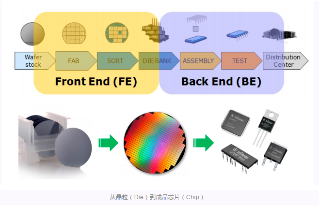
Next, we will provide a detailed introduction to the chip packaging testing process:
Wafer test
Before further processing, integrated circuit wafers must undergo rigorous testing to ensure the functional integrity of the die. The test divides the grains into three categories: Good Die with intact functionality, Defective Die with defects, and Fail Die with complete functional failure. According to the classification requirements for product shipment, we will select grains that meet the requirements for the next step of specific packaging production. This process is called CP testing, also known as Chip Probing Test, which involves testing the Pad pins of the chip by connecting probes to ensure its proper functionality. This step is crucial for ensuring the quality of the final product.
CP testing mainly relies on ATE testing equipment (i.e. Automatic Testing Equipment, abbreviated as ATE), probe station (i.e. Probe, a high-precision machine platform used to carry and move wafers so that the probe card probe can accurately contact and conduct with the die pad pin of the chip), and test probe card (i.e. Probe Card, a test board customized according to the circuit and testing requirements of each chip, used to achieve interconnection between ATE device channel resources and the corresponding pad of the chip) and other equipment and testing components. These devices and components work together to gradually complete the testing and verification of Die for each grain on the wafer. For problematic Dies, they are usually marked on their surface using methods such as "Ink" to facilitate selection and identification during subsequent packaging production processes.
Chip packaging
By conducting CP testing on IC wafers, subsequent packaging and production of functional grains can effectively avoid the cost loss caused by packaging defective chips. Although sometimes a "blind sealing" strategy is used, which encapsulates all grains on the wafer without CP testing and conducts testing and screening in subsequent stages. However, this method is usually limited to the initial engineering batch wafers after chip fabrication, with the aim of obtaining chip engineering samples as soon as possible to verify the success or failure of the chip fabrication, thereby saving project time. CP testing is an indispensable step when entering the mass production stage.
The chip packaging process varies significantly depending on the packaging form of the final product chip. Taking the common wire bonding process of solder ball grid array packaging (WB-BGA packaging) as an example, its production process covers the main process steps of chip packaging.
Wafer cutting is an extremely precise and demanding process technology aimed at dividing wafers that have undergone CP testing into independent grains. In this process, the first step is to conduct preliminary quality inspection on the wafer to ensure that it meets the cutting requirements. Subsequently, a protective blue film is applied to the front of the wafer to prevent damage to the grains during the cutting process. Depending on the packaging size and heat dissipation requirements, it may be necessary to thin the wafer by mechanical grinding to reduce its thickness. Subsequently, using diamond blades or laser cutting technology, precise cutting is carried out along the pre-set grooves on the wafer (i.e. wafer lines, which are reserved in the wafer manufacturing process to protect the grains during the cutting process). After completing this step, independent grains can be obtained. The wafer cutting process requires extremely high precision, and any minor process error may have a direct impact on the quality of the grains. Therefore, this process relies on professional production equipment - wafer cutting machines to complete. Globally, well-known wafer slicing machine manufacturers include DISCO and ACRETECH from Japan, as well as Slicingtech from the United States. In China, manufacturers such as Jingsheng Electromechanical and the 45th Institute of China Electronics Technology have also achieved significant success in this field.
In the process of manufacturing the final chip, the substrate (SUB) plays a crucial role. It is a special type of printed circuit board (PCB), whose key function is to extend and connect the Pad pins of die chips to the Ball pins after packaging. Therefore, SUB must be designed and manufactured based on the specific situation and packaging size of each chip. At present, well-known SUB manufacturers in the industry include Kyocera in Japan, South Asia in Taiwan, China, Xinxing Electronics and Jingshuo. In mainland China, companies such as Xingsen Technology, Zhuhai Yueya, Shennan Circuit, and Shengyi Electronics are also actively striving to break through the SUB production technology required for high-end chip packaging.
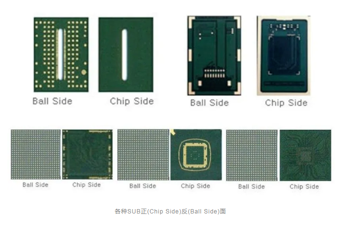
The substrate constitutes the basic structure of chip packaging, similar to the foundation of a building. Subsequently, the grain Die is precisely placed on one side of the substrate, a process known as Die Attach. The connection between the grains and the substrate is achieved through fine wire bonding technology. To ensure the stability and security of the chip, a metal protective cover will be installed on it, which is called Lid Attach. This protective cover is usually made of an alloy with excellent heat dissipation performance. On the other side, solder balls are installed on the chip, a process known as Solder Ball Mount. Subsequently, advanced reflow soldering technology is used to ensure a stable connection between the solder ball and SUB. At this point, the basic structure of chip packaging has been completed.
After packaging is completed, the chip will undergo strict quality inspection. This includes using techniques such as X-Ray to conduct detailed inspections of the internal structure of packaged chips to ensure packaging quality. In addition, marking operations will be performed to print the chip manufacturer's logo, product name, production batch, and other information on the chip surface through laser printing. After ensuring that all quality indicators are qualified, the chip will enter the baking process, also known as the Baking process. The purpose of this step is to eliminate moisture and other factors that may affect the performance of the chip packaging material, ensuring that the chip exhibits stable and reliable characteristics in subsequent electrical performance work.
After a series of meticulous packaging processes, the original wafer die is ultimately transformed into finished chip chips, laying a solid foundation for subsequent applications.
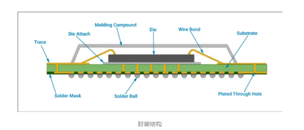
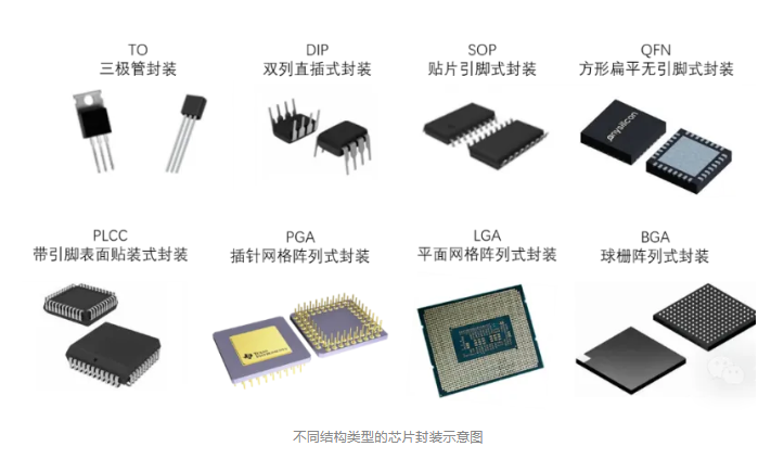
In addition to the traditional wire bonding BGA packaging method, the current mainstream is Flip Chip BGA, which is a reverse soldering packaging BGA. The reason why this method can achieve a smaller packaging size is because the chip is inverted and connected to the substrate. This technology first forms metal bumps on the wafer die pad through wafer bumping process, and then connects these bumps to the substrate below. By comparing the aforementioned methods, it is clear that there is a significant difference between the two. There are many types of chip packaging, and if classified according to the different packaging materials used, they can mainly be divided into plastic encapsulated chips, ceramic encapsulated chips, and metal encapsulated chips. Among them, the packaging of ceramic and metal materials is mainly used in aerospace and military fields with extremely harsh working conditions, and the packaging cost of these materials is relatively high. If classified by packaging structure, it becomes even more diverse, as different types of chips and application requirements require packaging forms with different structures.
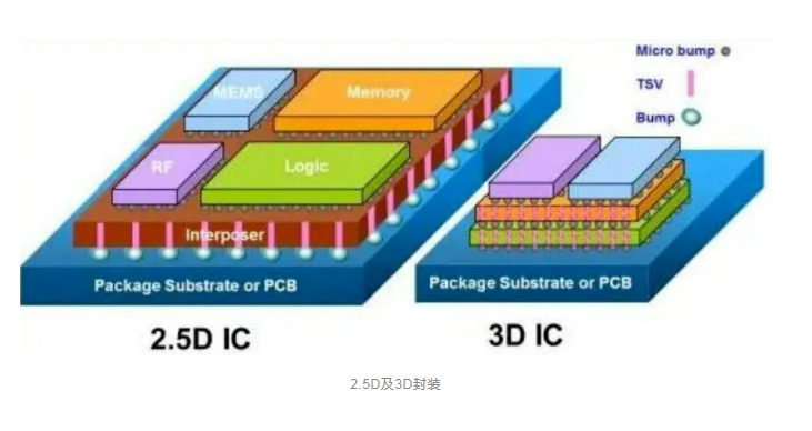
With the increasing demand for high-performance chips in the market and the expanding application areas of chips, packaging technology is also rapidly evolving. From the initial 2D packaging to 2.5D and even 3D packaging, the goal is to continuously improve chip integration through technological innovation. The currently highly anticipated artificial intelligence chips, namely AI SoC (System on Chip), require the integration and packaging of 2 to 8 or even more high bandwidth HBM storage chips (collectively referred to as KGD, which stands for Known Good Die). Therefore, higher requirements have been put forward for packaging technology. To ensure high-speed and stable interconnection bandwidth between HBM storage particles and main chip grains, the advanced CoWoS 2.5D packaging method has emerged.
Chip final testing
Before the chip is officially shipped and delivered to end product customers, in order to ensure its functionality and quality meet standards, it must go through a crucial testing process - Final Test. The necessity of this move stems from two reasons. Firstly, although CP testing can effectively evaluate chip performance, its testing power and frequency are limited by the way it contacts through probing probes at the wafer level. Secondly, during the packaging process, the chip may be damaged to a certain extent due to factors such as manufacturing processes. Therefore, conducting FT testing on the packaged final product is crucial as it can effectively identify and eliminate potential quality issues.
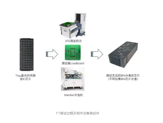
FT testing and CP testing are quite similar in testing methods, both relying on ATE automatic testing equipment. In addition, auxiliary tools such as a test board (Loadboard) and a sorting machine (Handler) are also required. These devices and tools together ensure the accuracy and efficiency of FT testing, providing solid quality assurance for the final shipment of chips.
System level testing
With the increasing size, functionality, and packaging technology of chips, their complexity is also constantly growing, which has led to a significant increase in the cost of CP and FT testing, and faces the problem of limited testing coverage. Especially in certain special fields where chip defect rates are extremely strict, such as autonomous driving chips, the requirements for testing quality are even more stringent. In order to effectively reduce the shipment defect rate, i.e. DPPM (Million Chip Failure Rate), many chips have added additional SLT testing (system level testing) after completing FT testing.
The design of SLT testing is based on the actual application scenarios of chips. By carefully creating test boards and developing testing processes, we strive to simulate the real chip business flow during the testing process. This testing method aims to ensure that the chip has passed strict inspections that are closer to the "actual application scenario" before being finally shipped to customers and applied to actual product boards, thereby reducing the DPPM defect rate to a lower level. This measure not only improves the quality of chips, but also enhances customers' confidence in the product. There is a close relationship between chip packaging and testing, so typical manufacturers in the industry chain are often referred to as packaging and testing factories. Shenzhen Zhongke System Integration Technology Co., Ltd. was established in 2011 and has been deeply involved in the field of advanced packaging for more than ten years, accumulating a wealth of experience in advanced packaging design simulation and process development. The company's main business includes wafer level packaging, IC test board design and processing, hardware design and development, and advanced packaging one-stop solutions. The company was fully acquired by Xinruiwei (Shanghai) Electronic Technology Co., Ltd. in 2021. Currently, as an excellent one-stop service provider for advanced system level packaging design in China, its products are widely used in many industries such as aerospace, vehicles, ships, communications, electronics, and healthcare.
Chip packaging and testing is an important link in the semiconductor integrated circuit industry chain, which is crucial for the physical shell protection, functional integrity, and performance reliability of integrated circuit chips. With the rapid development of technology, future packaging and testing technologies will continue to move towards miniaturization, high density, and high integration, such as using cutting-edge processes such as 3D packaging and wafer level packaging. These innovative technologies enable chips to achieve more diverse functions and excellent performance in a more compact space, thereby meeting the growing demand for chips in diverse application fields such as artificial intelligence, the Internet of Things, 5G communication, and automotive electronics. This not only promotes the vigorous development of the semiconductor integrated circuit industry, but also injects new vitality and opportunities into the entire technology industry.