Source: official account: semiconductor full solution
There are four main types of semiconductor device preparation and processing, namely:
(1) Graphic technology (photolithography)
(2) Doping technology
(3) Coating technology
(4) Etching technology
The specific processes include photolithography, ion implantation, rapid thermal process (RTP), plasma enhanced chemical vapor deposition (PECVD), sputtering, dry etching, and wet etching
(1) Graphic technology (photolithography)
Graphic technology generally refers to photolithography process, which is one of the most important driving forces for the rapid development of semiconductor technology, starting from the photographic plate making technology in printing technology
Photolithography technology enables people to present any pattern on a micro nano scale through photoresist, and when combined with other process technologies, transfer the pattern onto materials, realizing various designs and ideas for semiconductor materials and devices The light source used in photolithography technology has a direct impact on the accuracy of the pattern. The types of light sources generally include ultraviolet, deep ultraviolet, X-ray, and electron beam, and their corresponding pattern accuracy is improved in the order mentioned above
The standard photolithography process flowchart is shown in the figure, including surface treatment, homogenization, pre baking, exposure, post exposure baking, development, film hardening, and inspection steps

The surface of the substrate usually adsorbs H20 molecules from the air, which is detrimental to the lithography effect. Therefore, the substrate needs to be dehydrated first, which is baking
For substrates with hydrophilic surfaces, the adhesion between them and hydrophobic photoresist is insufficient, which can cause problems such as photoresist detachment or pattern displacement. Therefore, it is necessary to apply a layer of adhesive on the surface The currently widely used thickening agents are hexamethyldisilazane (HMDS) and trimethylsilyl diethylamine (TMSDEA)
After the surface treatment is completed, begin to evenly coat the photolithography limbs The thickness of the photoresist after uniform coating is not only related to the viscosity of the photoresist itself, but also affected by the rotational speed used during uniform coating. Generally, it can be roughly assumed that the thickness of the photoresist is inversely proportional to the square root of the rotational speed After the uniform coating is completed, it is necessary to evaporate the solvent of the photoresist through baking, which can further improve the adhesion of the photoresist. This process is called pre baking.
After all the above steps are completed, it is time to proceed to the exposure stage
There are two types of photoresist: positive photoresist and negative photoresist, and their properties after exposure are exactly opposite
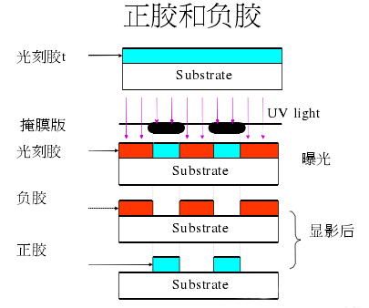
Taking photoresist as an example, unexposed photoresist is insoluble in the developer solution, but after exposure, it is easily soluble in the developer solution During exposure, the light source shines through a patterned mask onto the uniformly patterned substrate, causing the photoresist to be patterned and illuminated Normally, the substrate and mask need to be aligned before exposure to accurately control the exposure position When exposing, it is necessary to strictly control the length, as being too long or too short can cause distortion of the image After exposure, sometimes it is necessary to bake the substrate again to eliminate the influence of standing waves, but this step is not necessary and can be skipped for direct development The process of dissolving the exposed photoresist by placing the substrate in a developing solution is called development, with the aim of accurately replicating the pattern on the mask onto the photoresist The development time must also be strictly controlled. If the time is too short, the development will not be thorough, and if it is too long, the graphics will be distorted

Next is the hard film, which is further baked to make the photoresist film adhere more firmly to the substrate surface and increase the etching resistance of the film. The temperature of the hard film is generally slightly higher than the pre baking temperature
Finally, use a microscope to check if the graphics meet expectations After transferring the pattern onto the material through other processes, the photoresist completes its mission and needs to be removed There are two methods for removing glue: wet and dry. The former uses organic solvents with strong solubility (usually acetone) to dissolve the glue film, while the latter uses oxygen plasma to etch and remove the glue film
(2) Doping technology
Doping technology is also indispensable in semiconductor technology, as it can alter the electrical properties of semiconductor materials as needed There are generally two common doping methods, namely thermal diffusion and ion implantation
ion implantation
Ion implantation is the use of high-energy ions to directly bombard semiconductor substrates for doping Compared with thermal diffusion, ion implantation has many advantages The ions to be injected are screened using a mass analyzer to ensure high doping purity During the entire injection process, the substrate is generally kept at room temperature or slightly higher. There are many masking films available, such as silicon dioxide (SiO2), silicon nitride (Si3N4), and photoresist, which make the self alignment masking technique highly flexible The dose of ion implantation can be precisely controlled, and the distribution of impurity ions in the same plane after implantation is very uniform, resulting in high repeatability of the implantation results
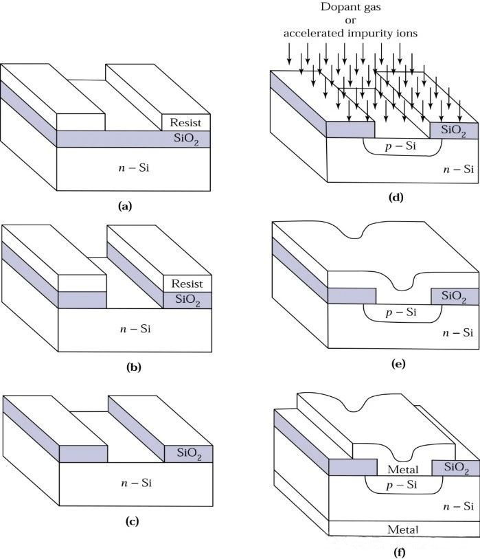
The depth of ion implantation is determined by the energy of the injected ions. By controlling the energy and dose of the ions, the distribution of impurity ions in the substrate after implantation can be controlled. Different implantation schemes can also be implemented multiple times in a row to obtain various forms of impurity distribution It is worth noting that in the case where the substrate is a single crystal, if the direction of ion implantation is parallel to the crystal direction of the substrate, a channel effect will occur, where some ions will move along the channel and the implantation depth will become difficult to control.
To avoid the occurrence of channel effect, the main axis direction of the single crystal substrate is usually deviated from the injection direction by about 7 °, or a layer of amorphous dielectric is covered on the surface of the substrate
Although ion implantation has many advantages, it also inevitably has disadvantages, such as severe damage to the crystal structure of the substrate After high-energy ions are injected into the interior of the substrate, they transfer energy to the atomic nuclei and their electrons through collisions, causing them to break free from lattice constraints and enter gaps, thereby forming gap vacancy defect pairs When the damage is severe, the structure of certain areas in the substrate crystal may be completely destroyed and become disordered amorphous regions
Lattice damage has a significant impact on the electrical properties of semiconductor materials, such as reducing carrier mobility and decreasing the lifetime of non-equilibrium carriers The most important thing is that the injected impurities are mostly located in irregular gap positions, which cannot form effective doping Therefore, after ion implantation, it is necessary to repair lattice damage and electrically activated impurities
Rapid Annealing (RTP)
Thermal annealing is the most effective method for repairing lattice damage and electrically activated impurities caused by ion implantation At high temperatures, the gap vacancy defect pairs in the substrate crystal will disappear due to recombination; The amorphous region also recrystallizes through solid-state epitaxy starting from the interface with the single crystal region To prevent the substrate material from being oxidized at high temperatures, the thermal annealing process needs to be carried out in a vacuum or inert gas environment Traditional hot annealing requires a longer time, which can lead to severe impurity diffusion and redistribution
The emergence of RTP technology has solved this problem, as it can greatly repair lattice damage and electrically activate impurities while shortening annealing time
According to different heat sources, RTP can be divided into the following types: scanning electron beam, pulsed electron beam and ion beam, pulsed laser, continuous wave laser and broadband incoherent light source (halogen lamp, graphite heater, arc lamp), among which broadband incoherent light source is the most widely used They can all heat the substrate to the desired temperature in an instant and complete annealing in a short period of time, effectively reducing the diffusion degree of impurities
(3) Coating technology
Plasma Enhanced Chemical Vapor Deposition (PECVD)
PECVD is one of the chemical vapor deposition (CVD) coating methods, in addition to two others, atmospheric pressure CVD (APCVD) and low pressure CVD (LPCVD)
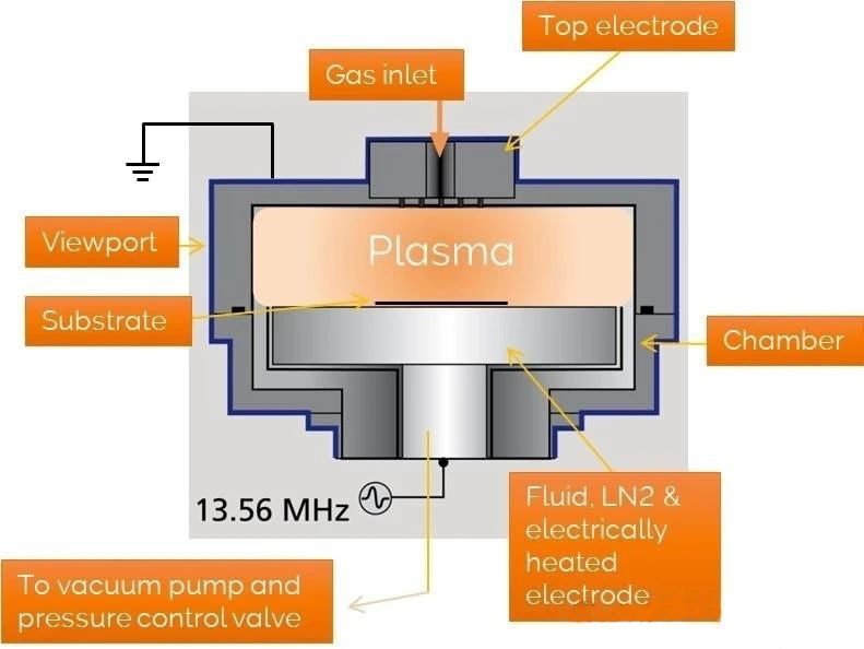
At present, PECVD is the most widely used of the three types. PECVD uses radio frequency (RF) plasma to induce and maintain chemical changes, and this chemical change can be carried out in non high temperature environments. Therefore, the film deposition temperature is low and the deposition rate is high. The equipment schematic is shown in the figure
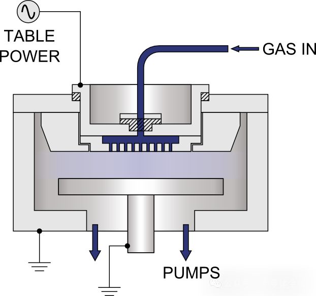
The thin film obtained in this way has outstanding adhesion and electrical properties, low microporous density, high uniformity, and strong small-sized filling ability The factors that affect the quality of PECVD coating include substrate temperature, airflow velocity, air pressure, RF power, and frequency
spatter
Sputtering is a physical vapor deposition (PVD) coating method Charged ions, usually argon ions (Ar+), have a certain amount of kinetic energy after being accelerated in an electric field. They are directed towards the target material and collide with target molecules, causing them to detach from the target material and be sputtered out These molecules also carry a certain amount of kinetic energy, moving towards the substrate and depositing on it

There are two commonly used sputtering power sources: DC and RF. DC sputtering can be directly applied to materials with good conductivity such as metals, while for insulating materials, coating can only be achieved through RF sputtering
The deposition rate of ordinary sputtering is low, the working pressure is high, and the quality of the deposited film is poor. The emergence of magnetron sputtering has ideally solved this problem It uses an external magnetic field to change the trajectory of ions from a straight line to a curve that spirals around the direction of the magnetic field, extending the trajectory of ions and improving the collision efficiency with target molecules, that is, increasing the sputtering efficiency, increasing the deposition rate, reducing the working pressure, and thus greatly improving the quality of the coating
(4) Etching technology
There are two types of etching methods: dry and wet. The former does not use a solution, while the latter uses a specific solution. The two etching processes are named after this
In general, a masking layer (which can be directly used as photoresist) needs to be prepared by photolithography before etching to protect the areas that do not require etching
Dry etching
The commonly used dry etching methods include inductively coupled plasma (ICP) etching, ion beam etching (IBE), and reactive ion etching (RIE)
In ICP etching, there are a large number of chemically active free radicals (free atoms, molecules, or atomic groups, etc.) in the plasma generated by glow discharge, which react chemically with the target material to produce volatile products, thus achieving the purpose of etching.
IBE is a physical process that uses high-energy ions (ionization from inert gases) to directly bombard the surface of the target material for etching;
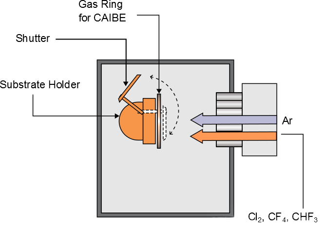
RIE can be seen as a combination of the previous two, by changing the inert gas used in IBE to the gas used in ICP etching, it becomes RIE
For dry etching, the vertical etching rate is much higher than the horizontal etching rate, that is, the aspect ratio is high, which can accurately replicate the pattern on the mask layer However, dry etching also has a certain etching effect on the masking layer, and the selectivity is poor in the ratio of the etching rate of the target material to the masking layer, especially for IBE, which may indiscriminately etch the entire surface of the material
wet etch
The method of achieving etching effect by placing the target material in a solution that can undergo chemical reaction with it (i.e. corrosive solution) is called wet etching
This etching method is simple to operate, low-cost, and has good selectivity, but the aspect ratio is very low, and the protected material below the edge of the masking layer will be corroded, which is not as accurate as dry etching To reduce the negative impact of low aspect ratio, it is necessary to choose an appropriate corrosion rate The factors that affect the corrosion rate include the concentration of the corrosion solution, corrosion time, and corrosion solution temperature
Reference: (1) Development and Optoelectronic Performance Study of Zhujiaqi Mid infrared Detector [D]; (2) Research on Key Detection Technologies for the Illumination System of Liu Zhifan's Deep Ultraviolet Lithography Machine [D]; (3) Research on the Preparation of Xu Jiajia InAs/GaSb Superlattice Long Wave Infrared Detector [D];
*Disclaimer: The content of this article is the author's personal opinion. Reproduction is only intended to convey a different viewpoint and does not represent the company's endorsement or support of that viewpoint. If you have any objections, please feel free to contact us.