Source: official account: Semiconductor Online
foreword
As the mainstream device of new power semiconductor devices, IGBT is widely used in various fields such as household appliances, electric vehicles, railways, charging infrastructure, charging piles, photovoltaics, wind energy, industrial manufacturing, motor drives, and energy storage.
IGBT module is a new generation of power semiconductor electronic component module, which was born in the 1980s and underwent a new round of reform and upgrading in the 1990s. Through the development of new technologies, IGBT modules have become a combination of many characteristics such as reduced on state voltage, fast switching speed, high voltage and low loss, and good high current thermal stability. These technical features are the main reason why IGBT modules have replaced old bipolar transistors as important electronic devices in circuit manufacturing.
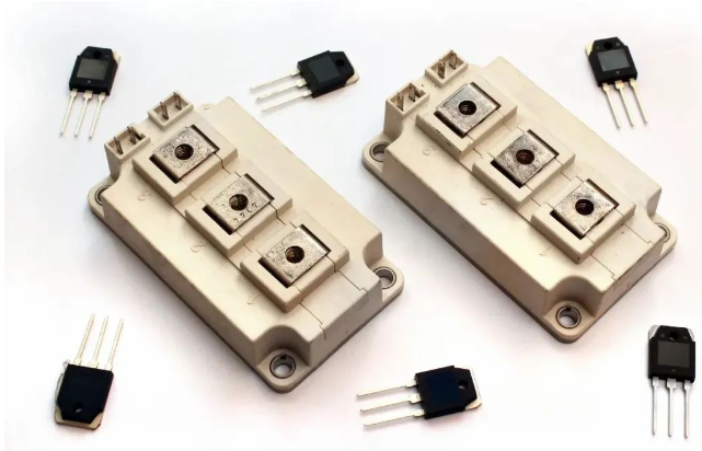
In recent years, the booming development of electric vehicles has driven the updating and iteration of power module packaging technology. At present, the power semiconductor technology of electric vehicle main inverters represents the advanced level of medium power module technology. High reliability, high power density, and cost competitiveness are the first requirements that need to be met.
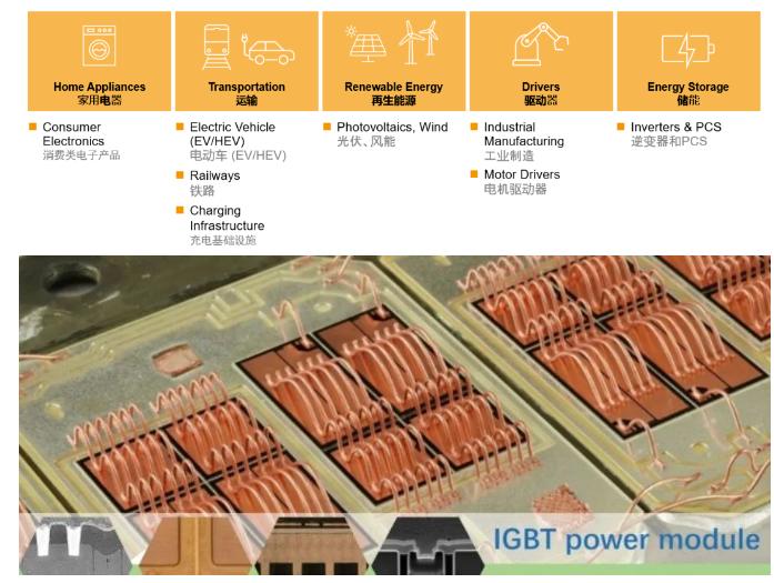
Evolution trend of power device module packaging structure
IGBT, as an important core component of power electronics, its reliability is the most important factor determining the safe operation of the entire device. Due to the adoption of stacked packaging technology in IGBT, this technology not only increases packaging density, but also shortens the interconnect length of wires between chips, thereby improving the operating speed of the device.
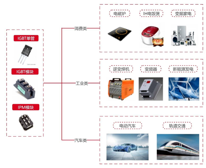
According to the packaging form and complexity, IGBT products can be divided into die DIE, IGBT single tube, IGBT module, and IPM module.
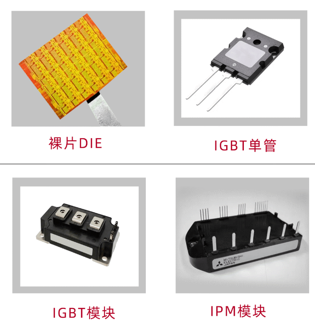
1. Die DIE: Multiple die DIEs cut from a single wafer;
2. IGBT single tube: a discrete IGBT device packaged with a single DIE, with low current capacity, suitable for home appliances and other fields;
3. IGBT module: composed of multiple DIEs packaged in parallel, with higher power and stronger heat dissipation capability, suitable for high-power fields such as new energy vehicles, high-speed railways, photovoltaic power generation, etc;
4. IPM module: an intelligent power module (IPM) that adds other functions around the IGBT module
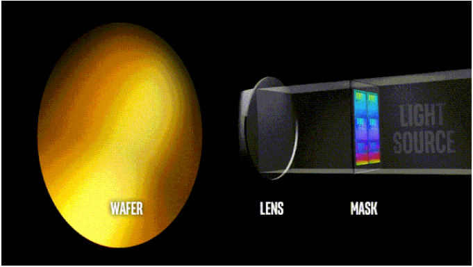
IGBT is known as the "pearl on the crown of power semiconductors" and is widely used in industries such as photovoltaic power generation, new energy vehicles, rail transit, distribution network construction, direct current transmission, and industrial control. The downstream demand market is huge. The core application product type of IGBT is IGBT module. The market share of IGBT modules can reach over 50%, while IPM modules and IGBT single tubes are only about 28% and 20% respectively. From the perspective of investment value of the product, IGBT modules have the highest value, which is beneficial for enterprises to quickly increase their product scale and therefore have the greatest investment value.
IGBT application fields

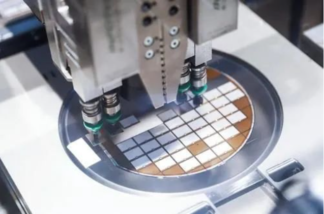
To achieve the localization of IGBT, it is not only necessary to develop a mature process technology that integrates chip design, wafer manufacturing, packaging testing, reliability testing, and system application, but also requires advanced process equipment.

With the development of chip thinning technology, higher requirements have been put forward for packaging. The packaging process is related to whether IGBT can form higher power density, be suitable for higher temperatures, have higher availability and reliability, and better adapt to harsh environments.
IGBT module packaging is the integration and packaging of multiple IGBTs together to improve the service life and reliability of IGBT modules. Smaller size, higher efficiency, and higher reliability are the market's demand trends for IGBT modules. There are many common module packaging technologies, and their names vary from manufacturer to manufacturer, such as Infineon's 62mm package, TP34, DP70, and so on. The packaging of an IGBT module requires production processes such as surface mounting, vacuum welding, plasma cleaning, X-ray inspection, bonding, glue filling and curing, molding, testing, and labeling.
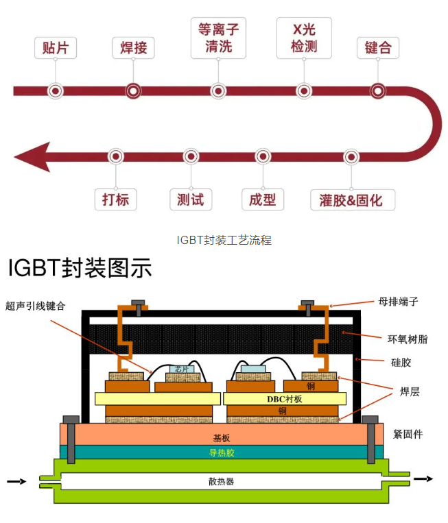
Introduction to IGBT module packaging process
1. Screen printing: Print solder paste onto the surface of the heat dissipation substrate and DBC copper plate according to the set pattern to prepare for the printing effect of automatic surface mounting;
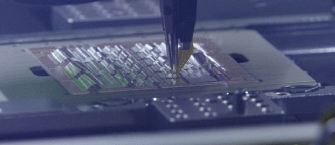
2. Automatic SMT: Attach IGBT chips and FRED chips onto the surface of DBC printed solder paste;
The IGBT packaging process includes screen printing, surface mounting, bonding, functional testing, and other processes. Any seemingly simple step in this process requires high-level packaging technology and equipment coordination to complete.
For example, in the SMT process, IGBT chips and FRED chips are mounted on the surface of DBC printed solder paste. This process requires the removal and placement of IGBT chips, and to ensure the yield and efficiency of surface mount, it is necessary for the surface mount machine with the motor as the core to have characteristics such as high speed, high frequency, and high energy control.
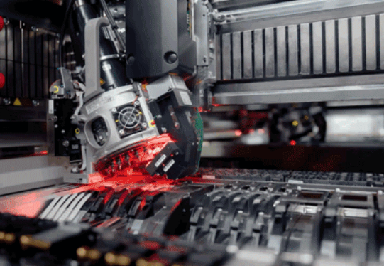
With the rapid development of the new energy vehicle industry, the demand for high-power and high-density IGBT modules has increased rapidly. Many car manufacturers have embarked on the path of IGBT self-developed to meet the needs of vehicle production and are no longer "stuck" by the upstream industry chain.
To produce IGBT modules with high reliability, high-precision chip mounting equipment is essential.
3. Vacuum reflow soldering: Place the DBC semi-finished product that has completed the SMT in a vacuum furnace for reflow soldering;
High quality welding technology is necessary to produce products with high reliability. Generally, reflow soldering furnaces will leave gas residues during the soldering process, forming bubbles and voids inside the solder joints. Excessive welding bubbles can have a negative impact on the reliability of solder joints, including:
(1) The mechanical strength of solder joints decreases;
(2) Reduced current paths for components and PCBs;
(3) The impedance of high-frequency devices increases significantly;
(4) Reduced thermal conductivity leads to excessive heating of components.
Vacuum reflow soldering is a reflow soldering technique that introduces a vacuum environment during the reflow soldering process. Compared to traditional reflow soldering, vacuum reflow soldering creates a vacuum environment in the later stage of the product entering the reflow zone. The atmospheric pressure can be reduced to below 5mbar (500pa) and maintained for a certain period of time, thus achieving the combination of vacuum and reflow soldering. At this time, the solder joint is still in a molten state, while the external environment of the solder joint is close to vacuum. Due to the pressure difference between the inside and outside of the solder joint, bubbles inside the solder joint are easily released, and the porosity of the solder joint is greatly reduced. A low void ratio is particularly important for power devices with large area solder pads. As high-power devices require conducting current and heat through these large area solder pads, reducing voids in solder joints can fundamentally improve the device's electrical and thermal conductivity.

4. Ultrasonic cleaning: Clean the DBC semi-finished product after welding with a cleaning agent to ensure that the surface cleanliness of the IGBT chip meets the requirements for bonding and wire bonding.
5. X-RAY defect detection: Screen semi-finished products with hole sizes that meet the standard through X-ray detection to prevent defective products from flowing into the next process;
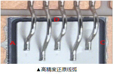
6. Automatic bonding: By bonding wires, IGBT chips or DBCs are connected together to form a complete circuit structure.
Semiconductor bonding AOI is mainly used for detection after WB section, which can provide solder, wire, solder joint, DBC surface for IGBT production
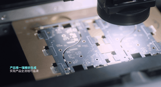
7. Laser marking: laser marking the surface of IGBT module housing, indicating product model, date and other information;
8. Shell plastic sealing: Glue the shell and install a bottom plate to bond the bottom plate;
9. Power terminal bonding
10. Shell gluing and curing: Add A and B glue to the inside of the shell and vacuum it, then cure at high temperature to achieve insulation protection;
11. Packaging and Terminal Forming: Installing a top cover on the product and bending the terminals into shape;
12. Functional testing: After conducting high and low temperature impact testing and aging testing on the formed product, the static and dynamic parameters of the IGBT are tested to meet the factory standard IGBT module finished product.
The packaging of power semiconductor modules is a crucial step in their manufacturing process, which affects whether power semiconductor devices can form higher power densities, be suitable for higher temperatures, have higher availability and reliability, and better adapt to harsh environments. The packaging technology characteristics of power semiconductor devices are compact and reliable design, and high output power. The key is to minimize the thermal resistance between the silicon wafer and the heat sink, and also to minimize the contact impedance between the input and output terminals of the module.
The packaging technology of IGBT modules is difficult, and high reliability design and packaging process control are its technical challenges. IGBT modules have the characteristic of long service life, and the service life of automotive grade modules can reach 15 years. Therefore, in the packaging process, modules have very high requirements for product reliability and quality stability. High reliability design requires consideration of material matching, efficient heat dissipation, low parasitic parameters, and high integration. Packaging process control includes low porosity welding/sintering, high reliability interconnection, ESD protection, aging screening, etc. A seemingly simple process in production often requires a long time of exploration to master proficiently, such as aluminum wire bonding. On the surface, only the circuit needs to be connected with aluminum wire, but the selection of bonding points, bonding strength, time, parameter settings of bonding machines, fixture design used in the bonding process, and employee operation methods can all affect the quality and yield of the product.
Disclaimer: This article is reproduced or adapted online, and the copyright belongs to the original author. The content of the article is the author's personal opinion. Reproduction is only intended to convey a different viewpoint and does not represent the company's endorsement or support of that viewpoint. If you have any objections, please feel free to contact us.