According to the application and manufacturing process of image sensors, they can be divided into CCD image sensors and CMOS image sensors.
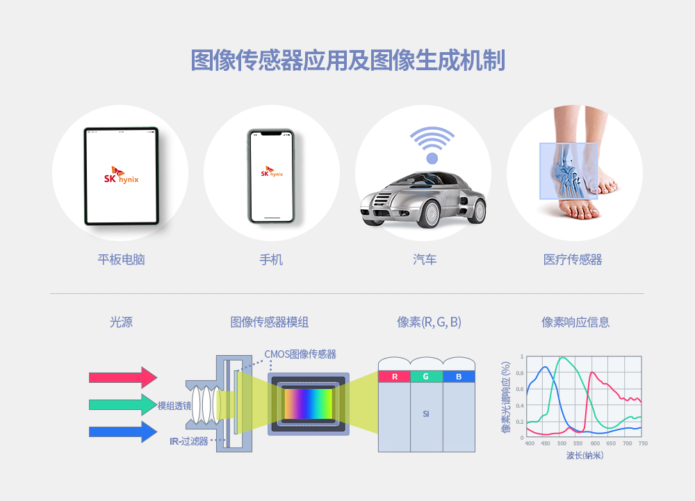
Especially CMOS image sensors (CIS) are not only installed in digital cameras, but also widely used in smartphones, tablets CCTV、 Various emerging market fields such as automotive black boxes, autonomous vehicle sensors, virtual reality (VR), medical equipment, drones, etc.

The working process of CMOS based image sensors is as follows:
When light energy in the visible wavelength range (400-700 nanometers) is concentrated in a photodiode (PD) on a silicon substrate, the silicon surface receives the light energy and forms electron hole pairs. The electrons generated in this process are converted into voltage through floating diffusion (FD), and then converted into digital data through analog-to-digital converter (ADC).
In order to manufacture CIS products that make this series of processes possible, it is necessary to adopt key manufacturing process technologies unique to CIS that are distinct from semiconductor memory. This type of process technology can be divided into the following five categories:
1. Deep layer photodiode forming process technology
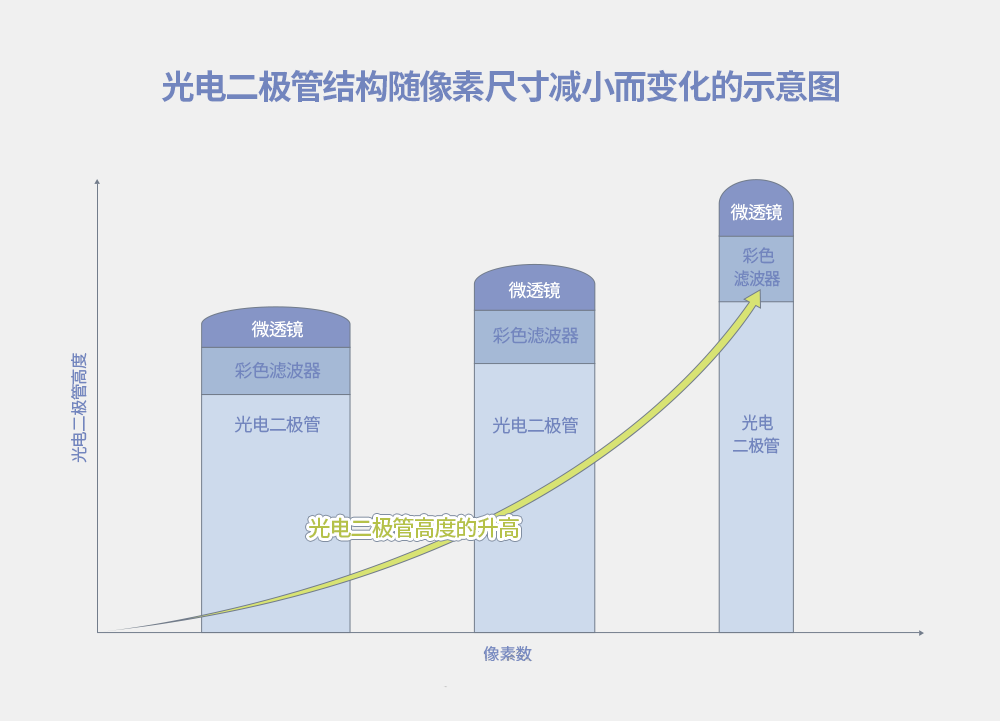
To increase the number of pixels on the same chip size, it is inevitable to reduce the size of a single pixel. The formation of deep photodiodes is a key technology to prevent a decrease in image quality. In order to ensure sufficient full well capacity (FWC) in smaller pixels, CIS requires more difficult image formation techniques compared to semiconductor memory. Especially, it is necessary to ensure high aspect ratio (>15:1) implant mask technology to prevent the implantation of high-energy ions; In fact, there is a gradual trend of increasing aspect ratio in the industry at present.

2. Pixel isolation processing technology
3. Color Filter Array (CFA) Processing Technology
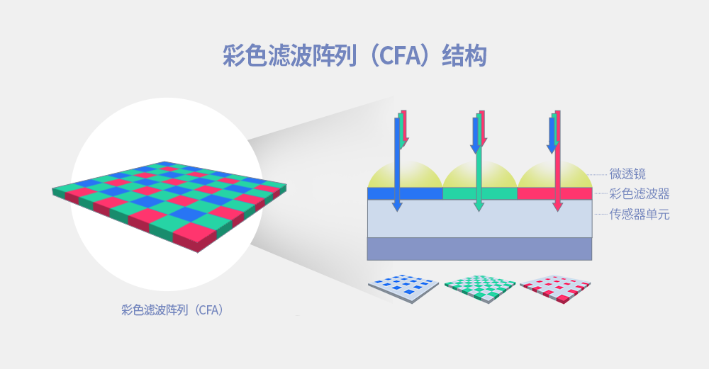
Color filter array is a unique CIS process distinct from semiconductor memory manufacturing technology. The CFA process generally consists of a color filter (CF) and a micro lens (ML). The former can filter incident light into various wavelength ranges of red, green, and blue, while the latter can improve light condensation efficiency. It is very important to develop and evaluate R/G/B color materials and develop related technologies to optimize process conditions such as shape and thickness in order to achieve excellent image quality.

4. Wafer stacking process
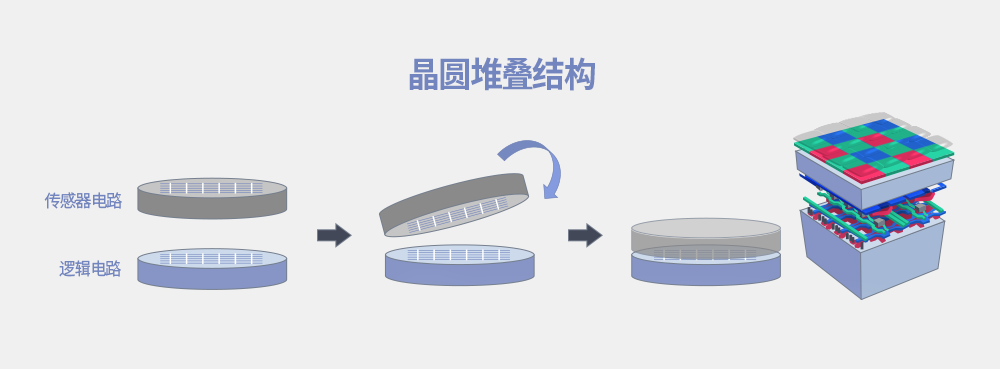
Wafer stacking refers to connecting two wafers together. This is an essential technology for producing high pixel, high-definition CIS products. For high pixel CIS products, pixel arrays and logic circuits are formed separately on individual wafers. These wafers are connected together during the manufacturing process, which is called 'wafer bonding'. The separation of pixel arrays and logic circuits means an increase in manufacturing costs, but it also means that more chips can be produced on the same wafer area; Not only that, but it also helps improve the performance of the product. Therefore, this is the technology currently adopted by most CIS chip manufacturers. Wafer stacking technology is constantly evolving in various forms. In recent years, wafer stacking technology has also been applied in the field of semiconductor memory, promoting the improvement of product performance.

5. Control technology that helps improve CIS yield and product quality
Controlling metal pollution is one of the most fundamental prerequisites in the development and mass production process of CIS products. Due to the sensitivity of CIS products to contamination being several times higher than that of memory products, and contamination directly affecting the yield and quality of CIS products, various pollution control technologies must be adopted in the production of CIS. Another important factor is plasma damage control. Due to the fact that damage to image attributes (such as thermal pixels) occurs during the manufacturing process, it is necessary to precisely manage critical processes.
Reference link: https://news.skhynix.com.cn/introducing_to_cis_key_process_technologies/
Disclaimer: This article is reproduced or adapted online, and the copyright belongs to the original author. The content of the article is the author's personal opinion. Reproduction is only intended to convey a different viewpoint and does not represent the company's endorsement or support of that viewpoint. If you have any objections, please feel free to contact us.