Dual pattern technology is a key technology for chip manufacturing that extends 193nm immersion lithography to critical dimensions<=45nm. Unlike nonlinear dual exposure technology, dual pattern technology does not have material and yield issues and has been widely used in advanced semiconductor manufacturing. Dual graphic technology uses different process techniques to achieve graphic transfer through single or two independent exposures. This technology can be easily promoted to triple or quadruple graphics technology, but it will increase costs.
Lithography Etching Lithography Etching
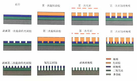
The most direct method is to transfer dense line patterns onto the substrate material by sequentially performing two independent photolithography and etching processes. The following figure shows the process flow of lithography etching lithography etching (LELE). The purpose of this process is to form dense line patterns on the silicon oxide layer of polycrystalline silicon wafers. Using a hard mask allows for easy transfer of graphics to the lower layer. The etching selectivity between the hard mask and the substrate material is usually significantly better than that between the photoresist and the substrate material. Inorganic hard mask materials such as SiN, SiON, and TiN can be deposited through chemical vapor deposition (CVD). Organic hard mask materials such as spin coated carbon (SOC) are polymers with high carbon content, which can be used as alternative materials to enhance planarization ability. Hard masks are not only used in LELE, but also commonly used in many advanced semiconductor manufacturing processes. The LELE process first performs spin coating and standard photolithography processes. The photolithography process generates a semi dense pattern in the photoresist, and then transfers the photoresist pattern onto a hard mask through etching. Next, peel off the photoresist and perform the second patterning process. The second graphical process also started with spin coating. The mask pattern used in the second photolithography is a mask pattern that has been offset in position, and a semi dense pattern is formed on the hard mask (in the photoresist) that has just formed the pattern. This pattern will be offset from the semi dense pattern generated by the first photolithography, doubling the density of the pattern on the hard mask. Peel off the photoresist, transfer the pattern on the hard mask to the underlying oxide layer, and complete the entire process

Lithography - Freeze - Lithography - Etching
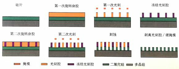
The Lithography Freeze Lithography Etching (LFLE) process is sometimes referred to as Lithography Hardening Lithography Etching (LCLE) or Lithography Lithography Etching (LLE). Compared with LELE, LFLE reduces one etching process and lowers costs. The typical process flow is shown in the following figure. This process first performs a standard photolithography process to form a semi dense photoresist line pattern. Unlike the LELE process, these photoresist line patterns are not transferred to the lower layer, but are subjected to special processing, namely freezing treatment. After freezing treatment, the photoresist lines are not sensitive to the second photolithography process. The freezing process uses surface curing agents or thermosetting photoresist. In addition, light with a wavelength of 172nm can also be used for pan exposure of certain photoresist materials to render them inactive. After the freezing step, spin coat the photoresist on the frozen photoresist again. Expose the newly spin coated photoresist, expose the offset line pattern inside the photoresist, and then develop it. The second photolithography process will not remove the photoresist frozen in the first step. In this way, the photoresist lines frozen for the first time and the photoresist lines developed for the second time form the mask used for subsequent etching processes. Transfer the pattern to the silicon oxide layer through etching process. Finally, peel off all the photoresist. LFLE has fewer process steps than LELE, resulting in lower cost and higher yield. Its requirements for design flexibility and etching control are similar to those of LELE. In actual manufacturing, it is necessary to comprehensively consider the mutual influence between the two photolithography processes of LFLE and between them and the freezing step. These mutual influences include: the scattering of light by the photoresist pattern formed by the first photolithography during the second exposure process, and the morphological changes during the first photoresist curing process; The influence of the photoresist pattern formed by the first photolithography process on the second photoresist spin coating process; The impact of the first photolithography and curing process on the performance of BARC; The second photolithography process causes partial deprotection and development reaction of the photoresist coated in the first spin coating; Mixing and diffusion between photoresists, etc.

Self aligning dual graphics technology
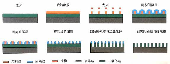
As shown in the figure below, Self Alignment Double Pattern (SADP) technology uses photoresist as a sacrificial layer to generate a pair of spacer layers on its left and right sides. Firstly, use standard photolithography techniques to create semi dense lines. Then, the spacer layer material (such as SiN) is uniformly deposited onto the photoresist through chemical vapor deposition (CVD). Subsequently, anisotropic etching was used to remove the spacer material. Except for the material attached to the sacrificial layer pattern side, all other spacer materials are etched and removed. Finally, selectively remove the photoresist material and etch the substrate using the remaining spacer layer as a mask. SADP only includes one photolithography step, so it will not be affected by the overlay error between two photolithography steps. However, the spacing between the spacer layer materials is influenced by the critical dimension (CD) of the sacrificial layer pattern (also known as the mandrel) and the uniformity of the sidewalls. The variation of the core axis pattern CD will change the period of the spacer layer pattern, and this phenomenon is called pitch walking. The process steps shown in Figure 5 can also be applied to sacrificial layer patterns with other geometric shapes. Forming spacer layers along the sidewalls of the core axis pattern formed by photolithography, and selectively removing certain spacer layer patterns through trimming exposure can improve design flexibility. The two SADP processes further reduce the period of the photolithography pattern. Using the spacer layer formed by the first SADP as the core axis layer for the second SADP can achieve self-aligned quadruple pattern (SAOP) technology.

Dual development technology
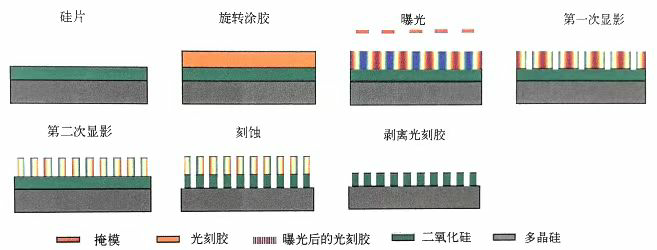
This technology develops the high-dose exposure area and low-dose exposure area of the photoresist separately, which can reduce the pattern period by more than half. The following diagram illustrates the basic principles of DTD. Expose photoresist using line blank patterns. The concentration of acid in photoresist is between the lowest value (blue) and the highest value (red); The first post baking (PEB, not shown in the figure) triggered a deprotection reaction, making the photoresist soluble in alkaline developer solution. Subsequently, the first positive development was performed, forming channels with the same period as the mask layout. The second development is negative development, using organic solvents to prepare staggered channel patterns. The etching process transfers the doubled frequency photoresist channel pattern to the lower layer, and finally removes the photoresist. DTD is another form of self-aligning dual graphics technology. The most attractive aspect of this technology is that the entire process can be completed on a coating and developing machine. Similar to SDDP technology, this technology is also limited by design graphics. The effect of DTD process is not only affected by the photoresist material, but also depends on the morphology generated after the deprotection reaction during the second post baking process. The second post drying occurs after the first positive development. Adding an overexposure process after the first development can improve the photoacid level and enhance the quality of the photoresist morphology after the second development. Although this technology has many attractive features, it is still only in the laboratory stage and has not yet been used in the commercial semiconductor manufacturing field.

The choice of dual or multiple graphics technology
The previous examples introduced several important dual pattern technologies that have been applied in semiconductor manufacturing. In addition, dual pattern technology also includes bipolar photoresist and self limiting acid diffusion period splitting technology. The process complexity of different dual and multiple graphics technologies varies, and their impact on chip design is also different. LELE and LFLE involve two photolithography exposures. Accurate alignment of the two exposed graphics is required. Due to the CD error caused by the overlay error between two photolithography processes, the dual pattern technology has increased the requirements for the overlay accuracy of the lithography machine. Although LELE and LFLE can be applied to more complex layouts, the difficulty of layout splitting is still significant. The interaction between dual graphics technology and optical proximity correction technology increases the complexity of chip design. Compared to other dual pattern technologies, LELE requires multiple photolithography and etching processes, which increases process time and cost. LFLE only requires one etching and all process steps can be completed on a coating and developing machine, but due to the need for two different photoresists, this technology adds process steps. These processes interact with each other and require accurate characterization and control. SADP/SAQP and DTD are both self-aligning dual pattern techniques that require only one photolithography exposure, reducing the requirements for overlay. These technologies will impose certain limitations on the design layout and may require additional exposures to form the final shape. The combination of SADP/SAQP and shear mask can be used to prepare logic circuit patterns, but it also increases the requirement for etching accuracy. SADP also requires logic circuits to adopt grid design, and graphics can only be in the same direction.
The requirements and compatibility of dual/multiple graphics technology for processes have been extensively validated and studied through experiments. The dual/multiple pattern technology, especially SADP/SADP and LELE, has been applied in advanced manufacturing processes. With the help of multiple pattern technology, DUV lithography can prepare patterns smaller than 20nm, but the process cost has also significantly increased, and the requirement for precision control of etching has been raised. At present, people have developed mathematical frameworks suitable for multiple exposure/graphic technology, which can only study overlay control and the effects brought by overlay. Combining dual pattern technology, EUV lithography technology can prepare patterns with feature sizes less than 10nm, further improving the level of advanced lithography technology.