Low cost lithography mainly refers to lithography techniques that do not require projection imaging, such as mask proximity lithography, laser direct writing lithography, and optical lithography without diffraction limits. Although the yield, resolution, and process control capabilities of these technologies are generally lower than DUV and EUV lithography, they are still widely used in the field of micro nano manufacturing. This article briefly introduces laser direct writing lithography technology.
Laser direct writing lithography does not require the use of masks, and can flexibly generate patterns of almost any shape using a simple focusing optical system. The price of laser direct writing system is much lower than advanced optical projection lithography, and its main drawback is that the serial writing method is very time-consuming and has low yield.
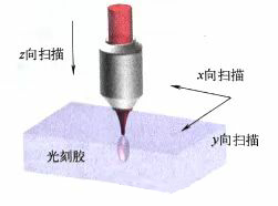
Laser direct writing (LDWL) uses one or more focused laser beams to expose photoresist. Control the exposure position of photoresist through the scanning motion of silicon wafers or laser beams. Micro nano structures can be manufactured on large areas exceeding a few millimeters using a workpiece stage and 2D scanning galvanometer. The worktable is generally a 3D linear piezoelectric sensor (PZT) driven worktable or a motor-driven worktable. The laser direct writing material processing technology (LDWP) that does not require photoresist also adopts a similar working principle. LDWL uses standard laser light sources. The light source of LDWP is a high-power femtosecond pulse laser, which can directly process materials. Early LDWL systems were mainly used for making photolithography masks and could serve as a cost-effective alternative to electron beam mask direct writing equipment. The exposure rate of a laser direct writing system depends on the shape of the focused beam and its scanning/motion on the photoresist. Laser direct writing lithography is generally used to prepare 2D or 3D graphics.

The following figure shows the intensity distribution or beam geometry cross-section of two types of laser direct writing beams. The plane wave passes through a focusing lens to form a sinc2 function (cylindrical lens) or Bessel function (spherical lens) intensity distribution with a waist. Due to the fact that the focusing lens can only collect partial plane waves, this structure can lead to overfilling of the pupil, low energy efficiency, and significant imaging sidelobes. Side lobes cause proximity effects, where adjacent diffraction patterns interfere with each other. Using a Gaussian beam with a very small beam width for illumination can ensure that most of the light energy can pass through the pupil. Using this configuration, the light intensity distribution on the pupil surface is Gaussian and will not be completely filled, making it the first choice for LDWL. When the NA is large, the shape of the focused beam is significantly affected by the polarization state.
The resolution of standard laser direct writing lithography is determined by the Abbe Rayleigh limit x=k1 * λ/NA, which depends on the exposure wavelength λ and the numerical aperture NA of the projection objective. The process factor k1 depends on the beam shape, photoresist, and other process conditions. The common value of k1 in laser direct writing lithography is about 1.0. The wavelength of most laser direct writing lithography systems is between 350-450nm, and the numerical aperture can reach 0.85. Therefore, the resolution limit of laser direct writing lithography is 300-500nm
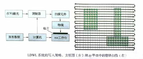
The scanning methods for focused laser beams include vector scanning and grid scanning. During the vector scanning process, the focused beam is moved to the desired exposure position for exposure. Typically, this method requires jumping the focused beam to different areas on the silicon wafer. It is very difficult to accurately locate the desired position in a short period of time. Therefore, most systems use grid scanning method. During the grid scanning process, the focused beam moves regularly along the rectangular grid.

The above figure is a schematic diagram of the basic writing strategy of mainstream laser direct writing lithography systems, which is the strategy of grid scanning on a straight grid. In this writing strategy, the focused laser beam moves on a uniform grid. Uniform grid is also known as addressing grid. Scanning actions can be performed by scanning components, such as moving the position of the beam focus through a mirror system, 3D displacement stage, or workpiece stage. Construct the desired image by scanning and adjusting the beam intensity simultaneously. In the simplest case, simply turn on and off the beam. By controlling the scanning motion and beam modulation through a computer, graphical data is input by the user. All discrete positions form an equally spaced addressing grid. The addressing unit is the distance between two adjacent grid points on the addressing grid. The number of points or pixels in the grid determines the writing speed of the laser direct writing device. When the addressing unit is small, it generates a large amount of graphic data, resulting in long write times; Larger addressing units can reduce data volume and write time, but will lower spatial resolution. The size and shape of the engraved light spot, the period/direction of the pixel grid, and the relative intensity between pixels and other exposure parameters determine the image quality of the rasterized graphics. Modifying computer image display technology and applying it to laser direct writing lithography can optimize and solve the contradictions in writing speed, grid image size, and accuracy. The use of rotating grids, grayscale pixels, and multi pass exposure methods can improve the minimum feature size, edge placement resolution and accuracy, CD uniformity, and edge roughness of imaging.
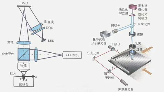
The use of raster scanning exposure method can more flexibly engrave graphics of any shape. However, the scanning time is relatively long, which limits the achievable yield. Maskless lithography combines the advantages of laser direct writing and optical projection lithography. The following figure shows a typical device for generating graphics using a digital micro mirror array (DMD) or other micro mirror arrays, which can dynamically adjust the geometric structure of the graphics. By adjusting the position and direction of individual micro mirrors in the array, the spatial and phase distribution of light can be modulated. The required intensity distribution can also be generated through liquid crystal display. The objective lens reduces the intensity distribution and images it into the photoresist on the silicon wafer. In short, the system can be seen as a projection lithography machine with programmable masks.

At present, the performance of optical maskless lithography cannot meet the requirements of advanced semiconductor manufacturing. Although the resolution of laser direct writing lithography is not as good as focused electron beam lithography, it is still widely used in the manufacture of low resolution lithography masks, printed circuit boards, and various research and development applications that require low cost and high design flexibility. Advanced commercial laser direct writing lithography machines use wavelength visible light (such as 405nm) and DMD to dynamically generate patterns, with resolution and yield that meet the requirements of many applications.
Reference: Advanced Semiconductor Lithography Process
Disclaimer: This article is reproduced or adapted online, and the copyright belongs to the original author. The content of the article is the author's personal opinion. Reproduction is only intended to convey a different viewpoint and does not represent the company's endorsement or support of that viewpoint. If you have any objections, please feel free to contact us.