Source: Content from Semi Dance
abstract
With the rapid development of industrial intelligent manufacturing and electronic information technology, the importance of integrated circuits is becoming increasingly prominent. Photolithography technology, as the core technology of the integrated circuit industry, has become a key research direction for domestic and foreign researchers. This article provides a brief introduction to photolithography technology and looks forward to future development directions. Firstly, the key indicators of the lithography system - resolution and its relationship with lithography performance were analyzed. Secondly, several commonly used exposure methods based on ultraviolet and deep ultraviolet light sources in the industry were discussed. Subsequently, the structure and performance of some representative lithography equipment were introduced. Then, the latest developments in EUV lithography and high NA lithography were summarized. Finally, the limitations of current photolithography technology were analyzed, and the future prospects of photolithography technology were discussed. This article aims to provide a guide for the use of lithography equipment, especially advanced products currently available. In addition, this article also focuses on introducing some challenges that photolithography technology may face in future development, and looks forward to the development trend of photolithography technology in the next decade, providing reference for guiding the future development direction of lithography machines and how to further promote Moore's Law.
introduction
In 1965, Moore hypothesized that the number of transistors that could be accommodated per unit area would approximately double every two years, which became an important law in the development of the semiconductor industry, known as Moore's Law. Over time, the entire semiconductor industry continues to develop under the guidance of Moore's Law. Photolithography technology is the core technology of the semiconductor industry, which determines whether Moore's Law continues to be effective. In the development of lithography machines, in terms of exposure methods, lithography machines started with contact lithography machines, went through proximity lithography machines, projection lithography machines, stepper lithography machines, step scanning lithography machines, immersion lithography machines, and now extreme ultraviolet (EUV) lithography machines. Researchers are constantly exploring how to apply shorter wavelength light on lithography machines to manufacture smaller on-chip circuits in exposure light sources. Firstly, in the 1980s, blue light with a wavelength of 436 nanometers (nm) emitted by mercury lamps was used as the light source for lithography machines, achieving a critical size of 1 micrometer. Subsequently, the wavelength of the light source reached 365 nm, known as the mercury i-line, pushing the feature size to 220 nm. In the mid-1980s, lasers began to be used and photolithography technology entered the deep ultraviolet (DUV) era. Deep ultraviolet lithography (DUVL) is playing an increasingly important role in the semiconductor industry. ArF excimer lasers with a wavelength of 193 nm and KrF excimer lasers with a wavelength of 248 nm are widely used as exposure light sources in industry [2]. F2 excimer lasers can provide light with a wavelength of 157 nm, but by 2003, due to limitations in photoresist and mask materials, 157 nm was considered the impractical next step in optical lithography after 193 nm [3]. Later, by introducing immersion solutions with a refractive index greater than 1, 193 nm immersion lithography replaced 157 nm lithography immersion lithography technology and brought projection optical systems with numerical apertures (NA) greater than 1. The NXT: 2050i produced by Advanced Semiconductor Materials Lithography Technology Company (ASML) is currently the most advanced DUV lithography machine using immersion lithography technology, with an NA of 1.35 and a resolution of up to 38 nanometers.
Although DUVL machines can reduce line widths to 7-5 nanometers through multiple exposure techniques, DUVL has reached its limit in order to achieve even smaller line widths. Extreme ultraviolet lithography (EUVL) using EUV as the light source has become a research focus, with a wavelength of 13.5 nanometers. ASML's EUVL machine NXE: 3600D can achieve a resolution of 13 nanometers and has the manufacturing capability of 5-3 nanometer logic nodes. As the next generation lithography technology, ASML and Carl Zeiss are developing a high NA EUV exposure system with NA=0.55 [5].
This article provides an overview of lithography machines and introduces the challenges they face. The rest of this article is arranged as follows. The second part will briefly introduce the basic principles of lithography machines, such as Rayleigh criteria and some relationships between parameters and lithography machine performance. The third part will introduce different types of lithography machines. The fourth part will showcase advanced EUV lithography machines and high NA EUV lithography machines, with a focus on light sources and optical components. The fifth part will analyze the limitations or technical issues of lithography machine research and provide future prospects.
principle
2.1 Resolution
Since the invention of integrated circuits in 1958, the integration density of integrated circuits has been continuously increasing, and the feature size has also been continuously decreasing. Up to now, the line width of integrated circuit graphics has been reduced by about 5 orders of magnitude, and the processing technology for line widths ranging from 28nm to 45nm has become very common. At the same time, the integration density has increased by more than 7 orders of magnitude, and a single integrated circuit chip can contain tens or even hundreds of millions of devices. These achievements are largely attributed to the advancement of photolithography technology. The lithography technology with a line width less than 1 μ m is already very complex technically, and further reducing the size of the lithography pattern on this basis will bring many technical and even theoretical challenges. At present, the primary issue to be addressed is how to further improve the resolution of photolithography.
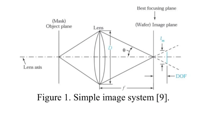
Resolution describes the ability of an imaging system to analyze the details of an imaged object. The minimum size of lines that can be distinguished and processed by a lithography system or the area that can be fully printed by the machine is called the minimum resolution for micro image processing. Resolution is one of the most important indicators of lithography systems, and the higher the resolution, the smaller the minimum line width that lithography can achieve. The Rayleigh formula is as follows

Among them, lm is the critical size, which is the minimum possible feature size. λ is the wavelength of the light used. K1 is a coefficient that depends on many other factors related to the chip manufacturing process. K1 is usually equal to 0.75, while the physical limit of photolithography is k1=0.25 [7]. NA is the numerical aperture of optical components, typically between 0.16 and 0.9. NA determines how much light they can collect, according to the following formula

N is the refractive index θ, which is the half angle at which the light cone converges into a point image on the wafer, D is the lens diameter, and f is the focal length [8], as shown in Figure 1 [9]. According to formula (1), resolution can be improved by reducing the wavelength λ (the limit of photolithography processing is λ/2, which is half wavelength resolution), increasing NA, optimizing system design (resolution enhancement technology), and reducing k1.
2.2 UV exposure
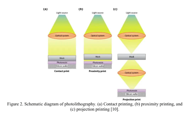
Ultraviolet (UV) and deep ultraviolet (DUV) light sources are currently widely used as exposure light sources in industry. The most common exposure methods using UV and DUV light sources are contact printing, proximity printing, and projection printing, as shown in Figure 2 [10].
2.2.1 Contact Printing
As shown in Figure 2a [10], in this technology, the silicon chip coated with photoresist is in physical contact with the mask. The chip is fixed by a vacuum system. When the chip comes into contact with the mask, the system is exposed to ultraviolet light from the top of the mask, and the exposure process occurs in the photoresist layer. Contact printing can achieve high resolution and is superior to adjacent printing because the photoresist and mask are in direct contact [11]. It was the first exposure method used in integrated circuit research and production, but it is now outdated due to dust being trapped between the photoresist. In addition, the mask template can damage the mask template and cause pattern defects, thereby reducing production. In addition, due to the direct contact between the mask and photoresist, it cannot be reused [11].
2.2.2 Adjacent Printing
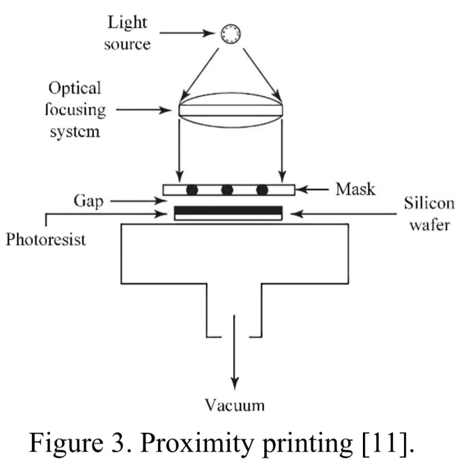
Adjacent printing is similar to contact printing. Figure 3 shows a schematic diagram of the adjacent printing system [11]. It consists of four main parts: light source and optical focusing system, mask, silicon wafer, and alignment stage. The optical focusing system converts the ultraviolet light emitted by the mercury lamp into parallel light, which passes through the mask and forms an image on the photoresist. Due to the small gap s (usually s=5 μ m) between the mask and the silicon wafer, this method is called proximity printing. In theory, the resolution of photolithography is 1/λ, but in proximity printing systems, the gap s between the mask and the silicon wafer is very small, which limits the resolution due to diffraction. In reality, proximity printing can only be used in processes above 3 μ m.
2.2.3 Projection Printing
Figure 4 is a schematic diagram of the projection printing system [11]. The optical focusing system converts the light emitted by the light source into parallel light, which then passes through the mask and is projected onto the wafer by the second optical focusing system. There is an alignment system between the wafer holder and the mask template. In fact, in order to achieve high resolution in projection printing, only a small portion of the mask is imaged. The image field of this small area is scanned on the wafer surface. The projection printer that steps the mask image onto the wafer surface with a resolution of a few nanometers is called a step repetition system [11]. The resolution of projection printing systems is mainly limited by diffraction, and generally speaking, projection printing can reach sub micron level.
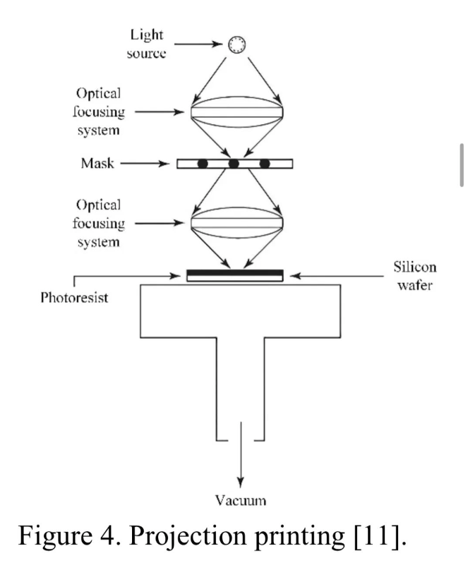
Projection printing has two most significant advantages. Firstly, the silicon wafer does not come into contact with the mask, avoiding process defects caused by contact wear. Secondly, the mask is not easily damaged and can be carefully corrected to eliminate defects and improve mask utilization. Due to these advantages, projection printing has become one of the most important methods for photolithography processes with a thickness of less than 3 μ m.
lithography gear
Since the invention of planar lithography technology, lithography equipment has gone through five generations, each of which can achieve a certain critical dimension (CD) and resolution. The representatives of the five lithography eras are contact lithography machines, proximity lithography machines, scanning projection lithography machines, step and repeat lithography machines, and step and scan systems.
3.1 Contact lithography machine
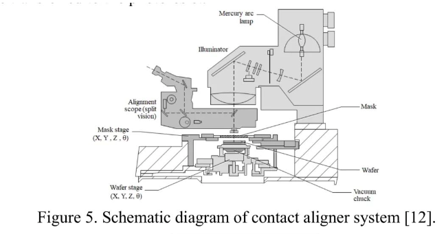
From the SSI era to the 1970s, contact lithography was the main method of lithography. It is used in manufacturing processes with a line width of 5 μ m or more. Although a line width of 0.4 μ m can also be achieved, contact lithography machines are no longer widely used. Figure 5 is a schematic diagram of a contact lithography system [12]. The mask template of the contact lithography machine contains all the array patterns that will be replicated onto the surface of the silicon wafer. The silicon wafer is coated with photoresist and loaded onto a manually controllable platform. Simultaneously observe the mask and silicon wafer through a spectrophotometer, and then manually position the platform to align the pattern on the mask with the pattern on the silicon wafer. Once the mask and silicon wafer are aligned, the mask will directly contact the photoresist coating on the surface of the silicon wafer, which is why the device is called a contact aligner. Then expose the mask and silicon wafer to ultraviolet (UV) radiation. Ultraviolet rays pass through the transparent part of the mask, and then transfer the pattern on the mask to the photoresist.
3.2 Proximity aligner
The proximity aligner was developed from the contact aligner and was widely used in the early stages of SSI and MSI in the 1970s. However, these aligners are still used in some small-scale production laboratories or old wafer production lines that produce discrete components, as investing in replacing old equipment with new equipment is not cost-effective. In actual manufacturing, this type of equipment is suitable for processes with line widths ranging from 2 to 4 μ m.
3.3 Scanning Projection Exposure Machine
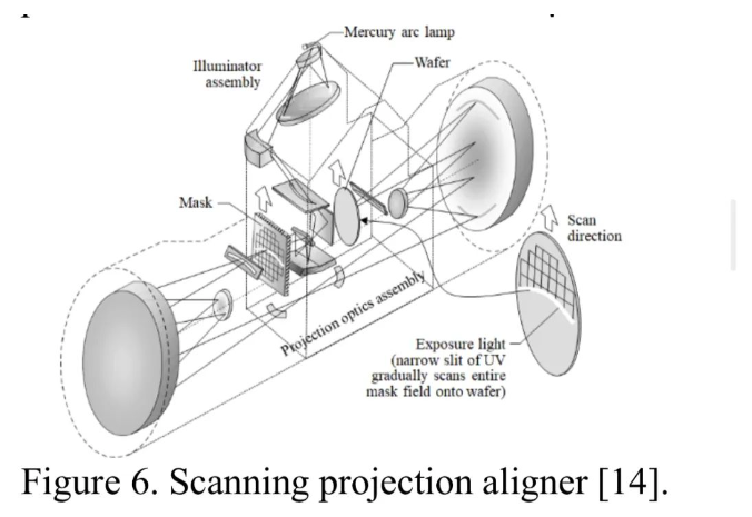
In the early 1970s, the development of scanning projection exposure machines (also known as scanners) attempted to solve the problems of contact exposure machines and proximity exposure machines mentioned earlier. In the late 1970s and early 1980s, scanning projection exposure machines were the dominant lithography exposure tools. These exposure machines are still used in old wafer production lines with a line width greater than 1 μ m. The concept of a scanning projection exposure machine is to use a reflection system to project the entire pattern on the mask onto the surface of a silicon wafer in a 1:1 ratio. Due to the 1X size of the mask, the image is not scaled, and the pattern on the mask is the same size as the pattern on the silicon wafer. As shown in Figure 6 [14], ultraviolet light is focused on the silicon wafer through a slit to obtain more uniform light. Place the mask template and the wafer coated with photoresist on the scanning frame and move them synchronously, then expose the photoresist on the wafer through a narrow ultraviolet beam. Finally, the image on the mask is accurately replicated onto the wafer surface through scanning motion.
3.4 Step by Step Repetitive Exposure Machine (Stepper)
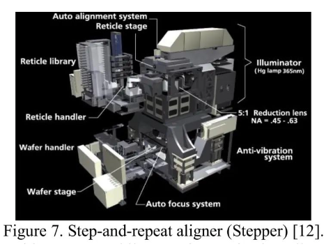
Stepper repeat exposure machine, also known as stepper machine, was the mainstream lithography equipment for silicon wafer manufacturing in the 1990s. The reason why the stepper repetitive exposure machine is named is because this device can only project one exposure field (possibly one or more chips on a silicon wafer) at a time, and then step to the next position on the wafer for the next exposure. In the late 1980s, stepper machines dominated the integrated circuit manufacturing industry. It is mainly used to form patterns with key dimensions as small as 0.35 μ m (traditional i-line photoresist) and 0.25 μ m (deep ultraviolet photoresist) [16]. Stepper lithography machines do not use photomasks, but instead use photomasks because photomasks contain patterns in a single exposure field corresponding to one or more chips, while photomasks contain all chip arrays. The optical projection exposure system of a stepper lithography machine uses refractive optical elements to project the mask image onto a silicon chip. Figure 7 shows the stepper repeat aligner [12].
Output is the main issue of stepper lithography machines. Scanning projection aligners can produce nearly 100 wafers per hour, while stepper lithography machines typically can only produce 20 to 50 wafers per hour. Formula (3) can be used to represent the output of the system:

Here, n represents the number of chips on each wafer, E represents the exposure time, M represents the time for the platform to move during each exposure, S represents the stability time of the platform, A represents the alignment time per field (if used), F represents the autofocus time (if used), and O represents the time including loading/unloading, pre alignment, moving wafers into and out of the system, and performing global alignment. In order to reduce or eliminate O, certain items in the total time can be completed simultaneously with the exposure of the previous wafer. Since n is usually between 50 and 100, the total time in parentheses in equation (3) is crucial for the commercial success of the stepper lithography machine. As a practical tool, it should be kept at 2 or smaller.
3.5 Step by Step Scanning System
In order to solve the contradiction between exposure field size and lens cost, with the development of lithography exposure equipment, the new technology of step scanning system has emerged. The step scanning system is a hybrid device that combines scanning projection exposure technology and step repetition exposure technology. It uses a reduced lens to scan the image of a large exposure field onto a part of a silicon wafer, and both the photomask and the silicon wafer are scanned by a narrowband focusing light. The standard exposure field size for the step scanning system is 26 mm × 33 mm, using a 6-inch photomask as shown in Figure 8 [17]. After the scanning and pattern transfer processes are completed, the silicon wafer will proceed to the next exposure area and repeat the scanning process.
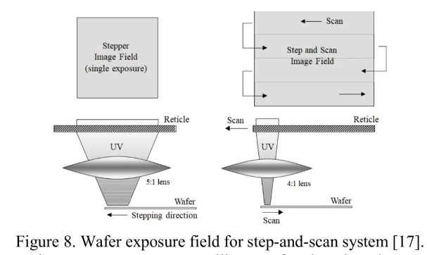
Using a step scanning system to expose silicon wafers has the advantage of increasing the exposure field, which can achieve larger chip sizes. The field of view of the lens can be just a thin strip, like a full wafer scanning projection aligner. Before advancing to the next position, it will scan a reduced mask (usually 4x) through a small and well calibrated 26 mm × 33 mm image field [13], as shown in Figure 9 [17]. Another significant advantage of a wider field of view is the ability to place more patterns on the mask, allowing for exposure of more chips in a single exposure.
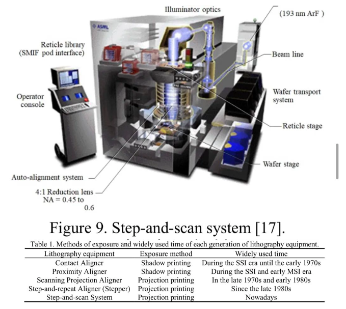
In addition, the step scanning system also has the ability to adjust the focus during the whole scanning process to compensate for lens defects and wafer flatness changes. This improves the control of the focus during the scanning process, thereby better controlling the CD uniformity of the entire exposure field. The main challenge of the step scanning system is the increased requirement for mechanical tolerance control, as the movements of the wafer stage and the mask stage must be synchronously controlled. The stepper machine only needs to quickly move the wafer to a new position, but the stepper scanning system must accurately move both the wafer and the mask in opposite directions simultaneously. During the scanning and stepping process, the positioning tolerance should not exceed tens of nanometers. Table 1 summarizes the exposure methods used by various generations of lithography equipment and their widely used time periods.
newest products
4.1 EUV Lithography Machine
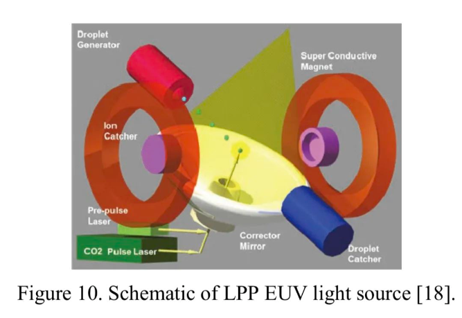
EUV lithography machine is an advanced lithography machine in the semiconductor industry, widely used in the manufacturing of chips with processes below 7 or even 5 nanometers. The core system of the whole machine is the exposure system. It produces EUV light. In order to achieve high efficiency, the system must be evacuated to prevent substances in the air from absorbing EUV. The laser generated plasma (LPP) source uses Sn droplets and a CO2 laser to generate 13.5 nm EUV light, as shown in Figure 10 [18]. When Sn droplets leave the generator, they will be "regulated" through pre pulses. The optimized Sn target has a lower density than the liquid target, so more Sn ions participate in EUV emission, thereby improving conversion efficiency [19]. We have achieved an EUV source power of 250 W [20]. The higher the EUV source power, the higher the throughput. For the lens, the high reflectivity mirror used in the exposure system will be absorbed when passing through the lens, which is attributed to EUV light, leading to a decrease in efficiency. In order to ensure transmission efficiency, the mirror is coated with multiple layers, essentially acting as a Bragg reflector [21]. ASML's advanced EUV lithography machine is NXE: 3600D, which uses EUV light with a wavelength of 13.5nm and a resolution of 13nm. The 3600D can be used to manufacture 5nm and 3nm logic nodes as well as cutting-edge DRAM nodes. The projection optical element has a diameter of 0.33NA. As for the production capacity, at a dose of 30mJ/cm2, it can produce 160 or more wafers per hour.
4.2 High numerical aperture EUV lithography machine
ASML and Carl Zeiss are developing the next generation EUV exposure system with NA=0.55 [22]. Compared with the 0.33NA lithography machine, the NA has increased by 67% and can provide sub 8 nanometer half pitch resolution [23]. For light sources, LPP light sources can still be used, but the power of the light sources used on EUV lithography machines is not sufficient to print smaller patterns. To achieve a 10 nanometer half pitch pattern, the dose should be greater than 80mJ/cm2 [24]. If the power of the light source is too low, the yield will significantly decrease. For high numerical aperture EUV lithography machines, a 500W light source with a dose of 80mJ/cm2 can produce 120 wafers per hour. If the power of the light source is high enough, the mechanical limit considered is 185 wafers per hour. When the power of the light source reaches 1.3 kW or higher and the dose is 80 mJ/cm2, this limitation occurs [25].
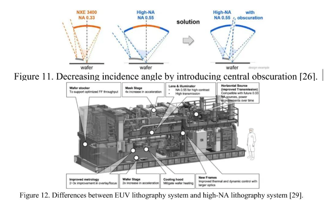
The increase in numerical aperture means an increase in deflection angle and an increase in the volume of the mirror. As the last mirror of a high numerical aperture optical system, according to the relationship of numerical aperture=nsin α, the cone angle of the light will increase from 19 ° to 33 ° compared to EUV lithography machines. For the second to last mirror, in order to avoid the last mirror being obstructed, the deflection angle should be increased and the volume of the mirror should also be increased. The multi-layer coating on the mirror acts as a Bragg reflector and must operate at a deflection angle to achieve maximum reflectivity with minimal angular changes. To solve the problem of how light can illuminate the last mirror at a smaller deflection angle, ASML introduced a central occlusion as shown in Figure 11 [26]. On one side of the mask, as the numerical aperture of the system increases, the numerical aperture will also increase. The incident light and reflected light will overlap during transmission. We have decided to adopt a 4x/8x deformation system to avoid contrast loss. But the exposure field will be reduced by half compared to the past [27, 28]. Figure 12 shows some other improvements of the high NA lithography machine compared to the 0.33NA lithography machine [29].
Limitations and Future Prospects
Under the guidance of the Rayleigh criterion, shorter wavelengths of light can be found, increasing NA and approaching the k1 limit more closely. Considering that the wavelength of EUV lithography light source is 13.5nm, it almost reaches the true X-ray wavelength range. Due to the strong penetration of X-rays into the reflective material on EUV lithography mirrors, the efficiency is low, resulting in very high X-ray losses. On the other hand, X-ray light sources imply higher power demands, which will bring new problems to power supply. Finding another shorter wavelength of light is more difficult than increasing NA. Another method of increasing NA is related to depth of focus (DoF). According to the formula of DoF,

Among them, k2 is a process related factor. As NA increases, DoF decreases. When k2=1, DoF is about 45nm, which is approximately one-third of the 120nm DoF of EUV lithography machines. To mask the defocusing of Airy spots, DoF control should be better than 35nm [20]. A lower DoF will pose new challenges to the flatness of the wafer surface, the thickness of the photoresist, and system control. A larger NA will result in a larger aperture of the reflector, making it larger and heavier, which is also an issue that cannot be ignored, bringing greater difficulties to manufacturing and assembly. Due to central occlusion, diffraction and some 0th or even 1st order diffraction points may be obscured [30], resulting in the loss of some pattern information and blurring.
The lithography machine is an extremely complex and precise system. To overcome technological limitations, it is necessary to consider using shorter wavelength light sources under the guidance of Rayleigh criteria to reduce the loss of short wavelength light during transmission. In terms of light sources, a free electron laser (FEL) is a type of light source suitable for photolithography. FEL has the advantages of continuously adjustable wavelength range, high output power, and high beam quality. EUV FEL and XFEL have great potential for application in lithography machines. However, the device used to generate FEL is quite large and expensive. The miniaturization of FEL devices and their application in industry remains a hot research topic. If FEL can be applied to the photolithography industry, higher power and shorter wavelengths will bring about increased productivity and finer patterns. In addition to the light source, optimizing the optical reflection system is also a necessary condition for making the structure more compact and saving costs. Increasing NA as much as possible may be easier than searching for shorter wavelength light sources. If the wavelength and NA of light are limited, adjusting k1 to achieve optimal performance is worth considering. High numerical aperture lithography technology is a powerful tool for continuing Moore's Law, but with the development of lithography machines, the challenges we face are not only mechanical limitations, but also physical limitations.
conclusion
In summary, this article discusses the characteristics of lithography machines from the perspectives of light sources and transmission systems. Specifically, an overall introduction to the lithography machine was first provided. Then, the key indicators of lithography systems - resolution - were discussed, as well as some common exposure methods developed on ultraviolet and deep ultraviolet light sources. Afterwards, for each generation of lithography technology, this article introduces a representative lithography equipment. Subsequently, we also summarized the characteristics of EUV lithography machines and the advanced development of high numerical aperture lithography machines. Finally, this article analyzes the limitations of current advanced lithography machines and outlines future prospects. Photolithography technology is the key to continuing Moore's Law, and high numerical aperture lithography machines have extended Moore's Law to the next decade. Looking to the future, it is necessary to consider feasible methods for the next era of photolithography to address the physical limitations that lie ahead of us. Overall, these results provide guidance for lithography machines, especially advanced products, while also presenting some viewpoints, pointing out potential challenges in the development of lithography machines, and proposing corresponding solutions.

Original English text:The Recent Progress of Lithography Machine and the State-of- art Facilities
*Disclaimer: The content of the article is the author's personal opinion. Reproduction on the website is only intended to convey a different viewpoint and does not represent the company's endorsement or support of that viewpoint. If you have any objections, please feel free to contact us.