Source:Optical Fiber Communication
The method of separating chips from wafers before packaging is called "semiconductor packaging". Like semiconductor chips, packaging is also developing towards the direction of "light, thin, short, and small". However, when connecting signals from inside the chip to outside the package, the package should not act as a hindrance. Packaging technology includes:
Internal Structure Technology;
External Structure technology;
Surface Mounting Technology (SMT).
Packaging development trend
To develop new semiconductor packaging, it is necessary to first change the installation method and external form of the packaging on the motherboard. Secondly, it is necessary to change the internal structure and materials of the packaging. As the packaging structure becomes more complex, the number of pins or balls soldered onto the motherboard increases, and the pin spacing decreases.
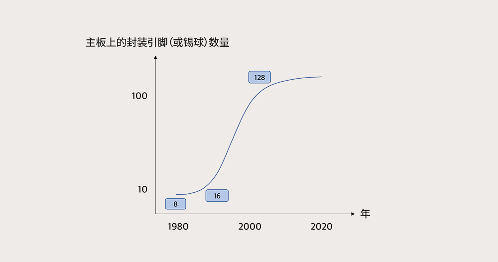
Changes in the number of semiconductor package pins (or solder balls) soldered onto the motherboard
At present, the number of contacts between the package and the motherboard has rapidly approached its limit and saturation point.
package structure
Semiconductor packaging includes semiconductor chips, carriers for loading chips (packaging PCBs, lead frames, etc.), and plastic packaging materials for packaging these devices.
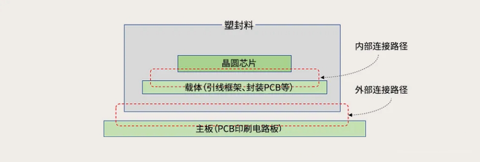
Internal and external structure of semiconductor packaging
In addition, internal and external connection paths are used to connect signals from the internal chip to the outside. Both internal and external connections used to be made using wires (wires or lead frames) in the past, but recently it has become common to use pads or solder balls. Meanwhile, plastic sealing materials play an important role in eliminating internal heat and protecting chips from external damage.
The three elements that determine the type of packaging: internal structure, external structure, and mounting
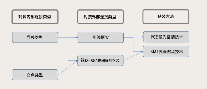
Schematic diagram of internal connection types, external connection types, and mounting methods for encapsulation
Until the late 1980s, the commonly used internal connection method for packaging was wire bonding, which used gold wires to connect chip pads to carrier pads. However, as the package size decreases, the volume occupied by the metal wires inside the package also increases.
To solve this problem, the metal wire was not removed, but instead a bump was used to replace the metal wire for internal connection. Of course, this does not mean that wire bonding methods are completely unusable. When using bump attachment, it is necessary to use bump attachment process and epoxy resin filling (Under Fill) method instead of die attaching and wire bonding process.
The external connection method has also been changed from lead frame to solder ball, because lead frame and wire have the same disadvantages. In the past, "wire lead frame PCB through-hole insertion" was used, but now the most commonly used is "ball grid array (BGA) surface mount technology"
Internal packaging type
Semiconductor packaging can also be divided into Wiring Type and Flip Chip Type based on internal structure.
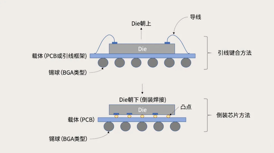
Comparison between wire bonding types and flip chip types
The lead method connects the chip upwards to the carrier through wire bonding. The flip chip method involves facing the chip downwards and connecting extremely small diameter solder balls (conductive metals called bump) to the solder pads. Therefore, the flip chip method does not require long wires to connect the semiconductor chip to the substrate, and has the characteristics of short signal transmission distance and strong adhesion. This can be considered an innovative technology to improve wire bonding defects.
The biggest advantage of flip chip is that it can reduce packaging size, improve power consumption and signal transmission process. Due to its shorter length, it is less affected by resistance and surrounding noise, resulting in faster speed. Therefore, the type of metal used for the bump material is also important. The most common ones currently are solder or gold. Another key point of flip chip is which epoxy resin to use to fill the gaps between the bumps and the carrier. In addition, flip chip does not use wires that occupy a large area, which can reduce the size of the formed chip. Therefore, it is widely used in small electronic devices such as mobile phones. That is to say, as the footprint area packaged on the motherboard decreases, it is more commonly used in high-density substrate technology. The emergence of small electronic devices such as smartphones has brought significant changes to packaging technology.
3D packaging technology: through silicon via TSV
To improve the density of chip packaging, we adopt multi-layer packaging by stacking multiple semiconductor chips. There are two types of multi chip packaging methods at the wafer level: wire bonding and through silicon via (TSV). TSV is a three-dimensional packaging technology that creates vertical vias between chips.

The three-dimensional packaging technology using through silicon chip via holes is shown in the figure
Silicon through holes are vertical through holes drilled in stacked chips and connected to signal lines through silicon through electrodes. Its advantages lie in fast signal transmission speed and high packaging density. Compared to two-dimensional packaging techniques that handle individual chips, through silicon vias (TSV) can be considered as three-dimensional packaging techniques.
If multiple layers of chips are connected by wires, a stepped stacked structure will be formed, which will increase the area by about twice. But through silicon via (TSV) can form a vertically stacked structure like an apartment building, requiring only about 1.2 times the chip area. Due to the higher space utilization efficiency of through silicon via (TSV) technology, its application scope is gradually expanding.
External packaging type and mounting method
External encapsulation type
There are various types of packaged chips. Taking the lead frame type as an example, there is a dipping type suitable for PCB through-hole insertion, which is developed in the order of SIP1, ZIP2, DIP3, and PGA4. However, due to its extremely limited ability to reduce the footprint of motherboard solder pads, it is currently only used in certain situations.
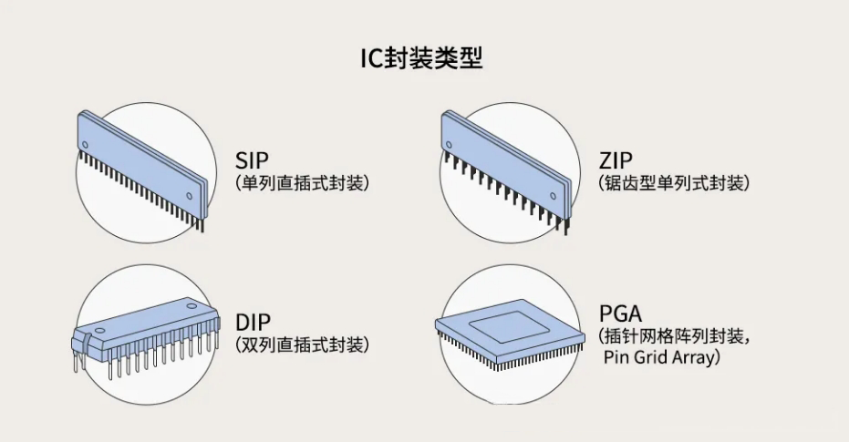
Image IC packaging type
There is also a type of Small Outline (SO) packaging technology in the lead frame category, which belongs to surface mount technology and improves integration by bending the leads. At present, it has been developed into SOIC and SOJ (J-type pin small form factor packaging) and widely used.
In addition, Quad Flat Package (QFP) is used on CPU chips. Subsequently, packaging technology changed from lead frame type to spherical, gradually giving rise to spherical contact array (BGA). At present, spherical shapes have become mainstream.
Mounting method
The packaging and assembly methods mainly include surface mount technology (SMT) and PCB through-hole insertion technology. As the name suggests, surface mount technology (SMT) is the process of fixing chips onto the surface of a motherboard through soldering, while PCB through-hole insertion technology involves inserting chip pins into the corresponding mounting holes on the motherboard and then soldering and fixing them to the motherboard's solder pads.
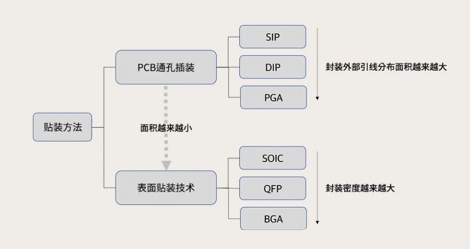
Image mounting method
However, due to the large area occupied by the mounting holes on the motherboard, in order to achieve a "lightweight and compact" packaging, the mounting method has developed into a hole free surface mounting technology. In the lead frame method, SO types (SOIC and SOJ) and TSOP were developed from the beginning for surface mounting. BGA type balls are designed to be mounted on motherboards, so surface mount methods are also applicable.
Disclaimer: This article is reproduced or adapted online, and the copyright belongs to the original author. The content of the article is the author's personal opinion. Reproduction is only intended to convey a different viewpoint and does not represent the company's endorsement or support of that viewpoint. If you have any objections, please feel free to contact us.