Source: official account: comprehensive research on optics and semiconductors
Extreme ultraviolet spectroscopy/soft X-ray electromagnetic radiation spectrum refers to the spectrum with a wavelength of 5-30nm. Similar to deep ultraviolet (DUV) lithography with exposure wavelengths of 248nm and 193nm, EUV lithography also uses a projection objective to shrink and image the mask. Due to the short exposure wavelength of EUV lithography, its resolution is significantly higher than DUV lithography. There are several important changes from DUV band optical lithography to EUV lithography: 1. High output power, long lifespan, and stable light sources are required. Various laser plasma or discharge plasma light sources have been developed in the industry. 2. Due to the lack of optical materials with sufficiently high transmittance in the EUV band, traditional transmissive lenses cannot be used in illumination/projection optical systems and must be replaced with reflective optical elements, which has a significant impact on the imaging characteristics of masks and EUV lithography systems. 3. We need photoresist materials with high sensitivity and resolution. High energy EUV photons alter the way incident light interacts with photoresist. Photon noise, secondary electron scattering effects, and other phenomena can all affect the sensitivity, resolution, and line edge roughness of photoresist.
The exposure wavelength of EUV lithography system depends on the light source and material, and the currently used wavelength is 13.5nm. The schematic diagram of the extreme ultraviolet projection lithography system is shown below. The collection mirror focuses the EUV light emitted by the laser plasma onto the relay focal point. The lighting system uses a four sided reflector to shape EUV light and illuminate the reflective mask on the mask stage. The projection objective system consists of six mirrors, which shrink the mask 4X and image it into the photoresist on the silicon wafer. Because all materials have insufficient transmittance for 13.5nm light, the system needs to operate in a vacuum environment.
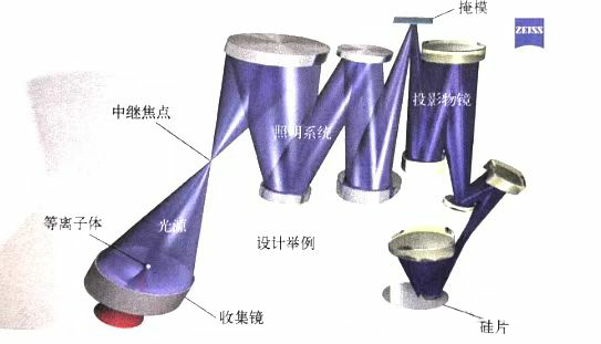
This article focuses on EUV light sources, multilayer mirrors, and high numerical aperture lithography. Multilayer mirrors are an important component of extreme ultraviolet lithography masks and imaging systems. The use of reflective masks and mirrors instead of transmissive masks and lenses has a significant impact on masks and imaging.
light source
The first EUV lithography experiment used a synchrotron free electron laser. Due to its low power and high cost, this synchrotron light source is not suitable for large-scale production. High energy electronic states in plasma can also generate EUV radiation. Plasma can be formed using target materials such as xenon, tin, and lithium. Both discharge plasma light sources and laser plasma light sources have been used in EUV lithography. The conversion efficiency (the ratio of EUV light power to input electrical or optical power within a narrow wavelength range) depends on parameters such as the target material, target shape, and plasma density. To achieve a conversion efficiency of 2% to 5%, newer light source systems commonly use tin as the target material. The following diagram shows the schematic of a discharge plasma (DPP) light source and a laser plasma (LPP) light source. The target material is transported from the tin cathode to between the cathode and anode of DPP through the feeding port or laser ablation technology. Plasma is generated through discharge (DPP) or high-power CO2 laser (LPP). The peak wavelength of the emitted EUV light is 13.5nm. Plasma also produces out of band (OOB) EUV radiation, as well as ultraviolet and visible light. The use of spectral purification filters such as thin films, multilayer mirrors, or special gratings can reduce out of band radiation entering the illumination system. Both DPP and LPP light sources produce high-speed moving debris such as particles/droplets, ions, and electrons. These debris may damage the optical components of lighting and projection systems. The foil trap can eliminate or reduce debris in the optical path. Multilayer films or grazing incidence collection mirrors reflect the cleaned EUV light to the relay focal point between the light source and the illumination system. The low conversion efficiency of DPP and LPP light sources indicates that most of the input power is converted into out of band radiation, debris, and heat loss, resulting in high thermal loads. How to effectively handle thermal loads has become a common challenge faced by these two EUV light sources. Debris can cause damage to the reflector and other light source modules around the plasma, seriously affecting the lifespan and stability of extreme ultraviolet light sources. The output power of EUV light sources is constrained by conversion efficiency, spectral filters, debris mitigation systems, and high thermal load processing methods. On the other hand, the yield index requires the minimum output power of the relay focus to reach 200W. The stability of the output power and the lifespan of the light source are also challenges faced in the development of EUV light sources. The above-mentioned issues and the insufficient performance of the light source have delayed the application of EUV lithography technology in semiconductor manufacturing for many years.

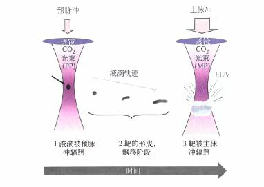
The extreme ultraviolet lithography machine adopts LPP light source and pre pulse technology, as shown in the figure. The function of pre pulse (PP) is to increase the volume of tin droplets and improve the interaction effect between tin droplets and main pulse (MP). The perfect spatiotemporal synchronization and pre pulse technology significantly improve the conversion efficiency, enabling the output power of EUV light sources to exceed 250W. Pre pulse technology is an important step in pushing EUV lithography technology into the semiconductor manufacturing process. In addition to the two types of light sources mentioned above, there are also other types of EUV light sources such as free electron lasers and resonant high-order harmonic lasers. Free electron lasers may be used as EUV lithography light sources in the future. High harmonic laser can be used for EUV metrology.
Multi-layer film reflection system
All materials within the EUV spectral range have similar optical properties and absorb EUV light, limiting the device's ability to manipulate EUV light. Refractive elements similar to lenses cannot be used in the extreme ultraviolet spectral range. The diffraction efficiency of diffraction elements such as transmission gratings, zone plates, or pinholes is low. Although they cannot be applied to high-yield lithography imaging systems, they can be used for metrology and some special applications. To achieve high reflectivity, it is necessary to use a large incident angle (grazing incidence mirror) or to enable constructive interference of reflected light from different interfaces of the reflective element (multilayer film mirror). The EUV imaging optical system and mask adopt a multi-layer film structure. The multilayer film is periodically stacked from bilayer films, as shown in the following figure.
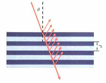
The Bragg theorem provides the conditions that need to be met for constructive interference of reflected light at different interfaces:

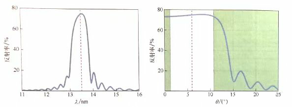
In the formula, d is the thickness of the bilayer membrane, λ is the wavelength, and m is an integer. The number of required double-layer films and the achievable reflectivity value depend on the difference in the real part of the refractive index between the two materials of the double-layer film. In order to make the difference in optical properties between the two materials large enough, double-layer films often use materials with high and low atomic numbers. When selecting materials, other technical requirements such as the manufacturing capability of continuous thin films with abrupt interfaces need to be considered. Currently, 40 pairs of double-layer films composed of molybdenum (Mo) and silicon (Si) are used in the mask. The refractive index contrast between these materials is high, and their absorption of EUV light is relatively small. The reflectivity of Mo/Si multilayer films can be calculated using the transfer matrix method. The following figure shows the variation curve of the reflectivity value of a typical Mo/Si multilayer film with wavelength and incident angle. At a working wavelength of 13.5nm and an incident angle range of 0 °~12 °, the theoretical reflectivity can reach about 70%. In the figure, the dashed line and the shaded area on the right represent the nominal wavelength, incident angle, and the range of incident angle corresponding to the numerical aperture of 0.33.
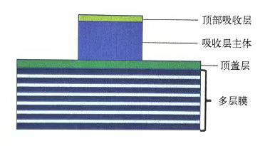
The absorption layer is located on top of the Mo/Si multilayer film and its main function is to generate EUV lithography mask patterns. The tilted illumination with an incident angle of 6 ° separates the reflected light from the incident light. The reflectivity of multilayer films varies with the incident angle and oblique illumination, resulting in several imaging phenomena unique to EUV lithography. The following is a cross-sectional view of a typical EUV lithography mask. 40 pairs of Mo/Si bilayer films were deposited on a substrate with ultra-low thermal expansion. In order to achieve high reflectivity within a certain range of incident angles, it is necessary to optimize the thickness of the Mo and Si layers. The thickness of the ruthenium cap layer is a few nanometers, which can protect the multilayer film from oxidation and other physical and chemical effects. The function of the absorption layer is to produce opaque patterns, usually composed of one or more materials. The chemical composition of the top absorption layer depends on the deposition process of the absorption layer and the interaction between the absorption layer and the local environment. The absorption layer film needs to be able to suppress the reflection of extreme ultraviolet light and facilitate the measurement and detection of masks using deep ultraviolet light.
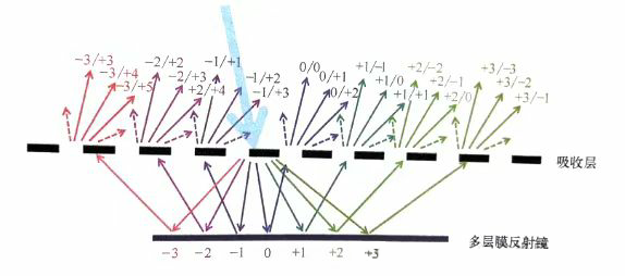
The following figure shows the diffraction process of light passing through an EUV mask. The figure shows the optical paths of each diffraction order propagating through the mask. The absorption layer and multilayer mirror are both simplified as infinitely thin optical elements. By setting the distance between the absorption layer and the multilayer film, the multilayer film is simplified as a reflective surface located within the real multilayer film. The light emitted by the light source propagates downward and diffracts upon reaching the absorption layer, forming discrete diffraction orders. The diffracted light shines onto the multilayer film, and all orders are reflected back to the absorbing layer. The upward propagating order is once again irradiated onto the absorption layer for diffraction. The light propagating upwards from the top of the absorption layer contains two sets of diffraction orders, representing the second diffraction of light. -The coherent superposition of diffracted light of orders 3/+3, -2/+2, -1/+1, 0/0,+1/-1... produces the 0th order diffraction within the pupil. The intensity of these diffraction orders varies, resulting in different phase delays when propagating between the absorbing layer and the (multilayer) mirror. The other diffraction orders within the projection objective pupil are also similar. The differences in propagation distance and phase delay between secondary diffraction and the effective reflection surface of the absorption layer and multilayer film result in some special imaging effects in EUV lithography that DUV lithography does not have.
EUV high numerical aperture lithography process
EUV lithography adopts a reflective projection system design, which requires a balance between imaging quality and light intensity transmission efficiency. Each multilayer mirror can only reflect about 65% of the incident light. Increasing the number of mirrors will introduce more optimization degrees of freedom, which is beneficial for improving imaging quality, but will reduce the system's light intensity transmission efficiency. Currently, the system with NA of 0.33 uses a hexagonal mirror. The following figure shows a design example of an EUV projection system. It can be seen that increasing NA has an impact on the silicon surface. After increasing NA, a larger (last) reflector is required. In the small NA system shown on the left and middle, the penultimate mirror tilts outward to the right, and the last mirror is illuminated by the penultimate mirror. Further increasing the inclination will result in a large range of incident angles of light on the last mirror, leading to severe loss of reflectivity.
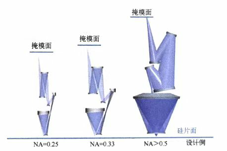
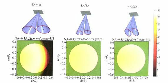
Therefore, the penultimate mirror of the high NA system did not tilt, but adopted a drilling scheme on the last two mirrors. These holes create a dark area or obstruction at the center of the projection pupil. The central obstruction only accounts for 4% to 6% of the pupil area, and it will not have a significant impact on imaging performance in practical applications. The following figure shows the impact of increasing the size of the imaging system by 4x on the mask surface. The numerical aperture of the mask/illumination surface is defined as NA (illu)=NA/M, where M is the magnification (reduction) factor of the projection system, usually 4. As shown in the left figure, in the system with NA=0.33, under oblique illumination conditions where the incident angle on the object side is the main ray angle (CRAO=6 °), the incident light and the mask reflected light can be separated. For a given system, increasing NA will result in a significant overlap between the incident light cone and the reflected light cone. This structure cannot separate the incident light and reflected light.
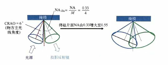
The first method to solve this problem is to increase CRAO to around 9 °. The larger CRAO and reflective mask increase the complexity of high NA EUV projection systems. As shown in the figure below, when the incident angle approaches the right edge of the projection objective pupil plane, the reflectivity of the multilayer film significantly decreases. At such incident angles, the decrease in reflectivity of multilayer films results in excessive contrast loss, especially for horizontally dense patterns. Changing the zoom ratio is a solution to avoid overlap between incident and reflected light in high numerical aperture EUV systems. The middle and right figures in the following figure show the system after changing the zoom ratio. The middle figure shows a system with a reduction ratio of 8 in both the x and y directions (8x/8x) and its corresponding reflectance map. The right figure shows the combined magnification system with a reduction ratio of 4 and 8 (4x/8x) in the non scanning direction and scanning direction, respectively, and their corresponding reflectance maps. Both systems have a larger reduction ratio in the direction of the main beam tilt. Within the effective incident angle range, the reflectivity of the mask multilayer film is almost the same. The change in magnification along the x-axis (perpendicular to the direction of inclination of the principal ray) has almost no effect on the reflectivity of multilayer films within the pupil.
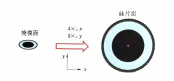
The application of combined magnification projection objectives has had a significant impact on both illumination systems and masks. In both the x and y directions, the shape of the lighting system and mask must be scaled according to the given ratio. As shown in the figure below, the object side elliptical illumination pupil is converted to a circular pupil in the image side. Combination magnification illumination can be generated by asymmetric field mirrors and corresponding asymmetric pupil mirrors.
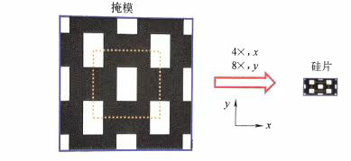
The following diagram shows the variation of the mask pattern from the object side to the image side. In practice, masks need to be made based on the stretched shape of the object. Due to the smaller line width, vertical patterns (along the y-direction) are more sensitive to mask morphology effects.
High NA systems emit light at a larger angle (image plane) and are more sensitive to polarization effects. The output light of EUV lithography plasma light source is non polarized light. The imaging contrast under non polarized lighting conditions is lower than that under optimized polarized lighting conditions. The refraction of light at the air/water/photoresist interface in DUV lithography reduces the impact of polarization on imaging. Unlike DUV lithography, the polarization effect of EUV light is almost the same in vacuum and photoresist (with a refractive index very close to 1). The interaction between EUV light and multilayer optical elements and masks can generate additional polarization effects. Understanding and handling related effects is crucial for driving high NA EUV lithography technology to its limits.
Disclaimer: This article is reproduced or adapted online, and the copyright belongs to the original author. The content of the article is the author's personal opinion. Reproduction is only intended to convey a different viewpoint and does not represent the company's endorsement or support of that viewpoint. If you have any objections, please feel free to contact us.